
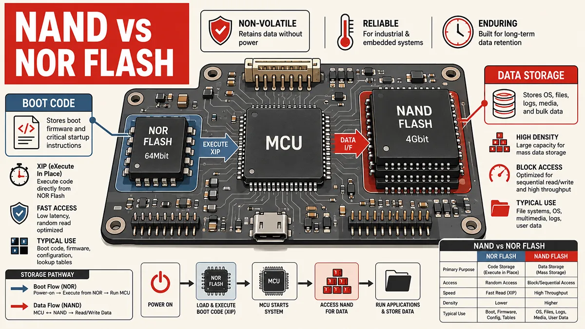
Flash memory fundamentally dictates the architecture of modern embedded systems and storage infrastructure. Deciding between NAND and NOR flash requires evaluating physical cell structures, access times, interface protocols, and lifecycle costs. This analysis provides an engineering breakdown of both non-volatile memory architectures to support hardware design and component sourcing decisions.
Quick Selection Guide
- Choose NOR Flash for boot code, firmware storage, XIP, low-density designs, and fast random reads.
- Choose NAND Flash for high-capacity storage, file systems, logging, and cost-sensitive data storage.
- Consider SPI NAND when capacity exceeds SPI NOR economics but board space and pin count remain constrained.
Basic Flash Memory Concepts and Terminology
To evaluate architectural differences, hardware engineers first establish a baseline understanding of non-volatile memory (NVM) operations and structural hierarchies. Both NAND and NOR utilize floating-gate metal-oxide-semiconductor field-effect transistors (FGMOS) or charge trap technology to retain electron states without active power.
The physical organization of these transistors defines the operational constraints. The memory array is subdivided into specific functional units:
- Cell: The base physical transistor storing one or more bits of data (SLC, MLC, TLC, or QLC).
- Page: The minimum granularity for reading and programming (writing) data in modern flash topologies.
- Block: A predefined group of pages that represents the minimum physical unit for the erase operation.
This asymmetry—where data can be read or programmed at the byte or page level but can only be erased at the larger block level—governs the write-amplification characteristics and firmware management requirements of the storage system. For authoritative definitions on these fundamental mechanisms, the Wikipedia article on Flash Memory provides a comprehensive historical and physical overview.
How NAND and NOR Flash Memory Work
The operational divergence between the two technologies originates at the silicon layout level. The way individual memory cells connect to the bitlines and source lines dictates the electrical behavior of the entire array.
What Is NOR Flash Memory
In a NOR flash architecture, individual memory cells are connected in parallel. One end of each cell connects directly to the source line, while the other connects to the bitline. This parallel arrangement behaves logically like a CMOS NOR gate. Because every cell has a direct electrical connection to the bitline, the memory controller can independently access specific bytes or words. This physical layout enables byte-level random access capabilities but requires distinct contact points for every cell, increasing the overall silicon footprint. Leading suppliers, such as Infineon (formerly Cypress), utilize this architecture for high-reliability components targeting industrial and automotive sectors.
What Is NAND Flash Memory
NAND flash memory organizes cells in a series configuration, resembling a CMOS NAND gate. A string of transistors (typically 32, 64, or 128) connects in series, meaning only the top and bottom cells of the string require contacts to the bitline and source line, respectively. This cascading structure reduces the required ground wires and bitline contacts, drastically shrinking the physical size of the memory array. However, this series connection limits access; the controller cannot read an individual byte without reading the entire series string. Consequently, data is accessed serially through page registers. Kioxia (the original inventor of NAND under Toshiba) pioneered this architecture to maximize storage density.
NAND vs NOR Flash Memory Core Differences
Beyond the physical layout, the architectural choices result in distinct system-level behaviors that influence MCU (Microcontroller Unit) integration and bill of materials (BOM) construction.
Addressing and Execute-In-Place Capabilities
The parallel nature of NOR flash provides a full address and data bus (in parallel implementations) or a highly optimized memory-mapped serial interface (in SPI NOR). This supports Execute-In-Place (XIP), a critical feature for embedded bootloaders. XIP allows the host CPU to fetch and execute instructions directly from the non-volatile memory array without shadowing the code into a separate SRAM or DRAM chip. The Texas Instruments application report on Booting and Flashing details how processors interface directly with NOR memory for immediate code execution upon power-on reset.
Conversely, NAND flash utilizes a multiplexed I/O interface where commands, addresses, and data share the same pins. It lacks a dedicated external address bus. A processor cannot execute code directly from NAND; the boot ROM must first shadow (copy) the operating system or application code from the NAND flash into system RAM before execution.
Key Factors Influencing Memory Cost
Silicon die area directly correlates with manufacturing cost. The parallel layout of NOR requires a cell size of approximately 10F² (where F is the minimum feature size of the lithography process). The series layout of NAND achieves a much denser cell size of approximately 4F².
As capacity requirements scale, this density disparity creates a widening cost gap. For low-density requirements (typically below 256Mb or 512Mb), SPI NOR remains cost-effective because it eliminates the need for external RAM and complex memory controllers. However, as system requirements approach 1Gb and beyond, the cost-per-bit of NAND becomes significantly lower, pushing engineers toward Serial NAND (SPI NAND) or managed NAND (eMMC/UFS) despite the added system complexity.
| Architecture Feature | NOR Flash | NAND Flash |
|---|---|---|
| Cell Connection | Parallel | Series |
| Addressing Method | Byte/Word Level (Direct) | Page Level (Multiplexed I/O) |
| Execute-In-Place (XIP) | Native Support | Not Supported (Requires RAM shadowing) |
| Relative Cell Size | Larger (~10F²) | Smaller (~4F²) |
Read Write and Erase Performance Comparison
Hardware selection requires matching the memory’s performance constraints with the host processor's workload profile. The architectural differences manifest in asymmetric read, program, and erase latencies.
NAND flash prioritizes block-level manipulation and high-throughput data streams. While its initial random read latency is high (typically 20 to 50 microseconds to fetch a page to the register), its sequential read throughput is massive once the page is loaded. Furthermore, NAND exhibits faster page program times (often under 500 microseconds) and block erase times (typically 1.5 to 3 milliseconds).
NOR flash excels in initial random access latency. A processor can read a byte from a NOR flash array in 50 to 120 nanoseconds, supporting immediate code execution. However, modifying data in NOR is computationally expensive. Byte or word programming takes significantly longer per bit compared to NAND page programming, and NOR sector erase times can range from hundreds of milliseconds to over a second, restricting its utility for frequent data logging.
Target Application Scenarios for Both Types
The electrical characteristics and cost structures align each technology with distinct industry use cases.
| Memory Type | Optimal Workload Profile | Typical Engineering Applications |
|---|---|---|
| NOR Flash | High read frequency, rare erase cycles, immediate boot requirements, low capacity (Mb). | BIOS/UEFI firmware, router operating systems, automotive ADAS boot code, medical device configuration data. |
| NAND Flash | High-volume data accumulation, sequential read/write, high capacity (Gb/Tb). | Solid State Drives (SSDs), smartphone storage, industrial data loggers, multimedia file systems (Linux rootfs). |
Engineering Component Selection Criteria
When transitioning from theoretical architecture to PCB layout, engineers must evaluate specific implementation requirements. Selecting a flash memory IC involves evaluating controller overhead, interface limitations, and data retention standards.
- Error Correction Code (ECC): NOR flash typically exhibits a very low bit-flip rate, allowing it to operate in many environments without complex ECC. Raw NAND flash expects bit errors over its lifecycle, requiring the host controller to implement robust ECC algorithms (such as BCH or LDPC) to ensure data integrity.
- Flash Translation Layer (FTL) and Wear Leveling: NAND blocks degrade after a specified number of Program/Erase (P/E) cycles. Engineers using raw NAND must implement an FTL in firmware to remap logical blocks to different physical blocks, ensuring uniform wear leveling and managing factory-marked bad blocks.
- Pin Count and Interfaces: Legacy parallel NOR and NAND consumed excessive MCU GPIO pins. Modern designs heavily favor the Serial Peripheral Interface (SPI). Quad-SPI (QSPI) and Octal-SPI (x8) NOR devices provide a balance of low pin count and high throughput, while SPI NAND provides a compatible package footprint for higher-density requirements.
Sourcing Electronic Components for Production Needs
Hardware design accounts for only half of the product lifecycle; supply chain stability dictates manufacturing viability. The memory semiconductor market is characterized by cyclical pricing, factory capacity shifts, and abrupt Product Change Notifications (PCNs).
Engineers and procurement teams frequently encounter End-of-Life (EOL) notices for legacy flash configurations. Migrating from a discontinued parallel NOR chip to a modern SPI equivalent, or finding a pin-to-pin compatible replacement across different fabricators (e.g., cross-referencing Winbond, Macronix, or Micron part numbers), requires rigorous datasheet analysis to verify timing requirements, voltage thresholds, and command set compatibility.
Optimize Memory Sourcing With Vigor Components
Mitigating supply chain volatility requires access to a stable procurement network and deep component intelligence. As a global independent electronic components distributor, Vigor Components assists engineering and procurement teams in navigating memory market fluctuations. Whether you need to locate allocated NAND flash inventory, secure EOL NOR flash for legacy industrial equipment, or evaluate pin-compatible alternative parts for a BOM cost-reduction initiative, Vigor Components provides actionable solutions. Visit Vigorcomp to search our global inventory network, access technical datasheets, and connect with our team to secure reliable memory components for your production runs.