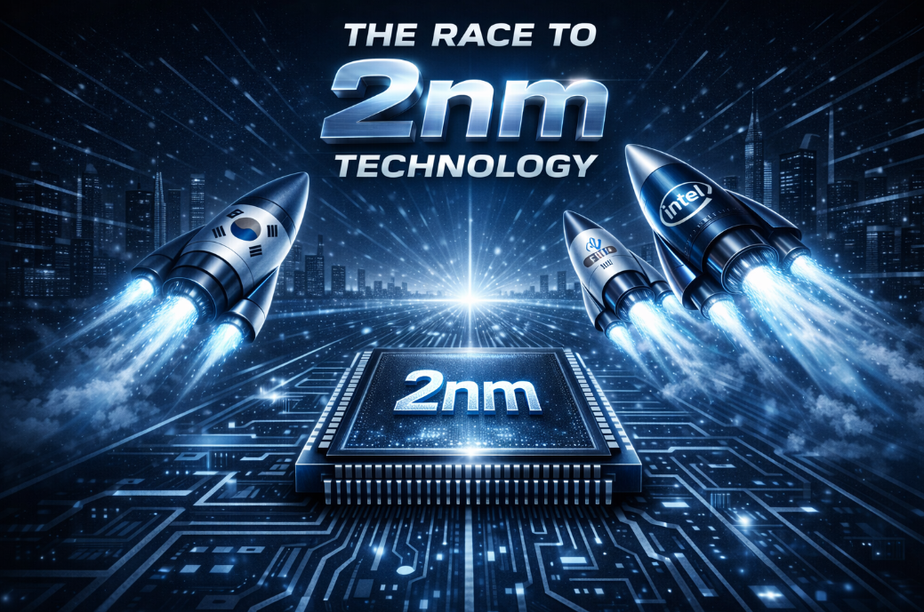
The global semiconductor industry is entering the 2-nanometer process era, driven by rapidly growing demand from artificial intelligence (AI), high-performance computing (HPC), and next-generation communication technologies.
Leading semiconductor players including Samsung Electronics, TSMC, Intel, and Japan’s emerging foundry Rapidus are accelerating investments and technological development to compete in this critical node of advanced semiconductor manufacturing.
Samsung: Bringing 2nm to Mobile Processors
Samsung has taken an early step in commercializing 2nm technology by introducing the Exynos 2600 processor, manufactured using a 2nm process node.
The chip adopts a next-generation Gate-All-Around (GAA) transistor architecture, delivering significant performance and efficiency improvements:
- Up to 12% performance gain at the same power level
- 25% lower power consumption at equivalent performance
- CPU performance improvements of up to 39%
- 113% increase in AI processing capability
Deploying the technology in its flagship smartphones allows Samsung to validate its advanced process in real-world applications while refining manufacturing capabilities for future large-scale production.
TSMC: Expanding Capacity for AI Demand
Driven by surging demand for AI chips, TSMC is rapidly expanding its 2nm manufacturing capacity.
The company is currently building new fabs in multiple locations in Taiwan and plans to further expand production facilities in Tainan Science Park. Construction of new facilities is expected to begin in 2026, aiming to address the growing demand for advanced semiconductor nodes.
Scaling production capacity will also help offset the rising manufacturing costs associated with leading-edge process technologies.
Intel: 18A Node for Next-Generation Servers
At MWC 2026, Intel showcased its upcoming Xeon 6+ server processor (codename Clearwater Forest) built on the Intel 18A process node—roughly equivalent to 1.8nm technology.
The processor leverages an advanced Chiplet architecture, integrating multiple compute tiles using Foveros Direct 3D and EMIB packaging technologies. A single processor can deliver up to 288 CPU cores, significantly enhancing computing density for data center workloads.
This approach reflects a broader industry shift toward advanced packaging and modular chip design to overcome scaling limitations.
Rapidus: Targeting Custom 2nm Manufacturing
Japan’s Rapidus is aiming to achieve 2nm mass production by 2027, with long-term plans to advance toward 1.4nm technology.
The company recently announced a collaboration with Canon and Synopsys to develop 2nm image-processing chips for advanced imaging devices. The project involves an investment of approximately JPY ¥40 billion, supported by government funding.
Rather than competing directly with large foundries across all markets, Rapidus is focusing on customized chip development for specialized applications, including imaging, AI, robotics, and high-performance computing.
Outlook
As 2nm process technology moves closer to large-scale production, the semiconductor industry is entering a new phase of technological transformation.
Innovations in transistor structures, chiplet architectures, and advanced packaging will continue to push the limits of performance and energy efficiency—powering future growth in AI infrastructure, data centers, 6G networks, and next-generation intelligent devices.
The race for advanced nodes will not only reshape chip design and manufacturing but also redefine the global semiconductor supply chain.