How Many IC Package Types Exist
There is no single fixed number of IC package types. If you classify packages only by how they attach to a printed circuit board (PCB), there are two broad mounting methods: through-hole and surface mount. If you classify them by familiar package families, you can name roughly nine or more common groups. If you count subfamilies, lead styles, body sizes, pin counts, materials, and manufacturer-specific outlines, the list can reach dozens or hundreds of variants.
That is why someone may say there are two types, another source may list nine, and a catalog may show 20, 45, or more entries. Those figures describe different levels of detail; they are not necessarily contradictory. The most useful question for an engineer or buyer is not "What is the universal total?" but "Which classification level helps me identify and specify the part correctly?"
For this guide, think in three layers:
Mounting method: through-hole or surface mount.
Package family: for example, DIP, SOIC, QFP, QFN, or BGA.
Exact variant: a particular lead count, pitch, body outline, height, terminal configuration, and manufacturer package code.
"Advanced packaging" is a useful discussion group for space-efficient or more integrated designs, but it is not a third mounting method. Many advanced packages, including chip-scale packages and wafer-level packages, also mount on the PCB surface.
What IC Packaging Is and Why It Matters
IC packaging is the structure that surrounds a semiconductor die and connects it to the outside world. Depending on its construction, it may use molded plastic, ceramic, a substrate, a lead frame, bonding wires, bumps, leads, or solder balls. The result is a component that can be handled, mounted, and connected to a circuit rather than an exposed die that is difficult to use directly.
A package serves several practical functions:
- Protects the semiconductor die: It helps protect the die from handling damage and environmental exposure during transport, assembly, and use.
- Provides electrical connections: It creates the electrical paths between the die and the PCB.
- Supports heat dissipation: It provides a path for heat to leave the device, although the final thermal result also depends on the PCB and surrounding system.
- Enables PCB mounting: It gives assembly equipment a defined mechanical shape and a terminal arrangement for attachment to the board.
- Adds mechanical protection: It helps safeguard the chip during handling and board assembly. However, a package does not make an IC immune to moisture, electrostatic discharge, or mechanical damage; handling and assembly requirements still depend on the specific device.
These functions affect more than appearance. Two ICs with equivalent electrical features can require different PCB footprints, assembly processes, and thermal designs if their packages differ. For design and purchasing teams, package identification is therefore part of selecting the right component—not an optional detail added after choosing the silicon.
Major Types of IC Packages
A practical classification tree starts with mounting method and then branches into families:
Through-hole packages: DIP and SIP have leads intended to pass through PCB holes.
Surface-mount packages: SOIC/SOP, SSOP/TSSOP, QFP, QFN/DFN, BGA, and LGA connect to surface pads, though their terminal structures differ substantially.
Advanced IC packages: CSP and WLCSP emphasize a package footprint close to the die size. These usually also use surface-mount assembly, so this branch overlaps with the one above.
The abbreviations below are family names, not complete specifications. A family can contain multiple pin counts, pitches, body dimensions, and manufacturer-defined outlines.
Through-Hole Packages
DIP and SIP
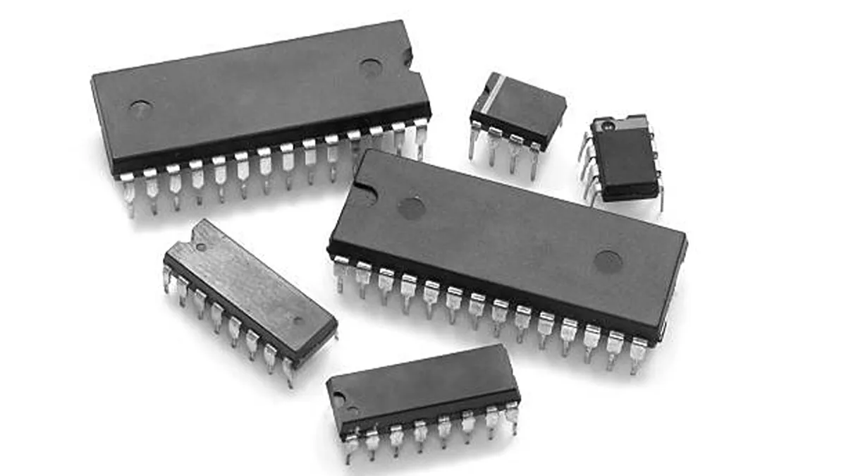
A dual in-line package (DIP) has two parallel rows of leads. Its accessible pins and compatibility with sockets make it convenient for some prototypes, test setups, and legacy equipment. A single in-line package (SIP) has one row of leads and appears in certain specialized or older designs. Both use drilled PCB holes, so they generally consume more board area or constrain routing differently than compact surface-mount options.
The name alone does not establish an exact footprint. A DIP with a different pin count, row spacing, or body width may need a different PCB pattern or socket. When maintaining an existing assembly, confirm the drawing rather than assuming all DIPs with similar markings fit.
Surface-Mount Packages
SOIC, SOP, SSOP, and TSSOP
These small-outline families place leads along two opposite sides of the package. SOIC is a common small-outline integrated-circuit style, while SOP is a broader small-outline package name used somewhat differently across manufacturers. SSOP and TSSOP describe more compact variants with finer leads and, in the case of TSSOP, a thin body profile.
Compared with through-hole parts, these packages usually make denser surface-mount layouts possible. Visible side leads can also make solder-joint inspection and some rework more approachable than packages whose connections sit entirely underneath. However, a narrow-body SOIC and a wide-body SOIC are not automatically footprint-compatible, and SOIC, SSOP, and TSSOP should never be treated as interchangeable based only on pin count.
QFP, LQFP, and TQFP
A quad flat package (QFP) has outward-bending leads on all four sides. Low-profile QFP (LQFP) and thin QFP (TQFP) are related forms distinguished by their specified outlines and heights. The four-sided layout supports more terminals than a typical two-sided small-outline package while leaving the leads visible after assembly.
QFPs appear in many microcontrollers and other devices that need numerous connections. Their fine-pitch leads require careful placement and can bend during handling. The PCB designer must check the exact lead pitch, body size, lead span, and pin-one orientation before assigning a footprint.
QFN and DFN
A quad flat no-lead package (QFN) has peripheral terminals around four sides of its underside; a dual flat no-lead package (DFN) typically places terminals along two sides. Neither relies on projecting gull-wing leads. Many, but not all, versions have an exposed center pad that can provide a useful thermal path into the PCB when the board is designed and soldered accordingly. Texas Instruments provides application guidance showing that QFN thermal performance depends on the exposed pad, PCB copper, and thermal-via design.
These families can save space and reduce the length of some electrical paths, making them attractive for compact power-management, RF, and mixed-signal designs. The trade-off is that most solder connections cannot be checked as easily by direct visual inspection. Footprint, stencil, and rework planning become particularly important.
BGA and LGA
A ball grid array (BGA) uses an array of solder balls beneath the package. By distributing connections across the underside rather than only around the perimeter, it can support many connections without requiring an extremely long row of fine-pitch outer leads. BGAs are common where connection density matters, including some processors, programmable logic devices, and memory products.
A land grid array (LGA) has flat lands instead of preattached solder balls. Depending on the device and application, an LGA may solder directly to a board or mate through an appropriate socket or contact system. That difference is significant for assembly and sourcing: "LGA" does not by itself tell you whether a particular board needs reflow or a socket. Both BGA and LGA require close attention to pad layout, underside terminal mapping, inspection capability, and rework method.
Advanced IC Packages
CSP and WLCSP
A chip-scale package (CSP) is a size-oriented category: its package footprint is close to the dimensions of the die. Wafer-level chip-scale packaging (WLCSP) creates the package-level interconnections while devices are still in wafer form, yielding a particularly compact finished component. CSP and WLCSP describe a packaging approach, not a separate PCB mounting method.
Small size can help in tightly packed products, but the reduced pitch and limited accessible area can complicate PCB fabrication, assembly, inspection, and replacement. Designers should not select a WLCSP solely because its outline appears smallest in a catalog. Board-level reliability, routing rules, and the manufacturer's recommended land pattern matter just as much.
Common IC Packages Compare
The table is a screening aid, not a substitute for a specific package drawing. Pin counts and pitches vary widely within a family; thermal performance also depends on die size, exposed pads, board copper, vias, and airflow. For example, a TI comparison of one 56-pin QFN against selected leaded packages shows advantages for that design, but TI explicitly notes that system-level results depend on board construction and operating conditions.
| Package family | Mounting method | Terminal layout | Typical pin count | Pitch | PCB space | Thermal performance | Assembly difficulty | Inspection | Rework | Common applications |
|---|---|---|---|---|---|---|---|---|---|---|
| DIP / SIP | Through-hole | Two rows / one row of projecting leads | Usually low to moderate | Often relatively coarse | Usually high for DIP | Device- and board-dependent | Accessible for manual assembly; holes required | Leads and joints generally visible | Often straightforward, especially if socketed | Prototypes, sockets, legacy boards |
| SOIC / SOP | Surface mount | Leads on two sides | Usually low to moderate | Often coarser than SSOP/TSSOP | Moderate | Depends on body and board design | Conventional SMT assembly | Outer joints visible | Usually manageable with suitable tools | Analog ICs, logic, drivers |
| SSOP / TSSOP | Surface mount | Finer leads on two sides | Low to moderate | Generally finer than standard SOIC | Low to moderate | Depends on device and board design | More sensitive to alignment and solder bridging | Outer joints visible but small | More delicate than larger SOICs | Interface ICs, control and analog circuits |
| QFP / LQFP / TQFP | Surface mount | Leads on four sides | Moderate to high | Often fine | Moderate; requires perimeter clearance | Depends on pad and board layout | Fine-lead placement and handling needed | Perimeter joints generally visible | Possible but lead damage is a concern | Microcontrollers, controllers, programmable devices |
| QFN / DFN | Surface mount | Flat peripheral pads underneath, on four / two sides | Low to moderate, sometimes higher | Often fine | Low | Can be strong with a correctly designed exposed-pad heat path | Stencil and reflow control important | Most joints hidden or only partly visible | Needs controlled heating and pad preparation | Power management, RF, compact controllers |
| BGA / LGA | Surface mount or specified socket for some LGA designs | Ball / land array underneath | Moderate to very high, depending on device | Array pitch varies by design | Efficient for dense connections; routing may need more layers | Highly package- and board-dependent | Requires process control and appropriate board design | Hidden joints may need X-ray or other suitable inspection | Specialized equipment and process often needed | Processors, FPGAs, memory, dense ICs |
| CSP / WLCSP | Usually surface mount | Compact underside contacts, often an array | Device-dependent | Often very fine | Very low package area; routing can be demanding | Strongly design-dependent | Fine-pitch placement and board controls needed | Joints generally hidden | Often difficult on dense boards | Space-constrained portable electronics |
"PCB space" should include routing and keep-out needs, not only the plastic or silicon outline. Similarly, a package that is easy to place in volume production may be inconvenient for a one-off laboratory repair. Use the table to narrow options, then compare manufacturer drawings and assembly notes for the actual candidates.
How to Identify IC Package Types
Start with observable features, then confirm them against manufacturer documentation. A visual match narrows the possibilities; it does not prove the exact package code or device identity.
Check lead arrangement and shape. Are there one, two, or four rows of external leads? Are the terminals projecting pins, bent gull-wing leads, or flat pads near the underside edges?
Check the connection position. A grid of underside solder balls suggests BGA; underside flat lands suggest LGA; perimeter pads on the bottom point toward QFN or DFN. The package may need magnification or an underside view to distinguish them.
Read the top marking and pin-one indicator. Markings can be abbreviated, especially on small packages. Record the logo, characters, date or lot information, and orientation, but do not assume the top text is the full manufacturer part number.
Find the exact manufacturer part number. Look up the ordering-code suffix and the manufacturer's package code. Those identifiers can distinguish otherwise similar package offerings; they may also encode temperature grade, finish, or shipment format, so decode them using that manufacturer's documentation.
Compare the dimensional drawing. Verify body length and width, maximum height, lead span, pitch, terminal dimensions, and the recommended PCB land pattern. Analog Devices, for example, provides a package index organized by drawing or package code, pin count, outline drawing, and land pattern.
Names such as SOIC-8, QFN-32, and LQFP-64 usually use the trailing number to indicate the number of leads or terminals, not the body dimensions. A "QFN-32" label alone does not tell you whether the body is square or rectangular, which pitch it uses, or whether it has an exposed pad. For a closer look at package-size labels and drawing measurements, see our article "What Do the IC Dimensions Numbers Mean?".
A useful real-world check is Vigorcomp's listing for STM32F103R8T6, which describes the device as a 64LQFP part. That description identifies a family and terminal count, but it is still the manufacturer's exact ordering information and package drawing—not the abbreviated listing alone—that should control footprint approval.
How to Choose the Right IC Package
Choose a package by working backward from the product's constraints and the manufacturer's available versions of the IC. A package is not "best" in isolation; it is a trade-off among layout, heat, assembly capability, serviceability, and cost.
PCB space and routing: Check the complete land pattern and escape-routing area. A physically smaller BGA or WLCSP can still demand finer fabrication rules or additional PCB layers.
Pin count and connection layout: Match the required signals, power pins, and grounds to a package the device actually offers. A higher pin count is useful only if the board can route it reliably.
Thermal requirements: Review power dissipation and the manufacturer's thermal data under relevant test conditions. If the design relies on an exposed pad, provide the specified copper area and thermal-via strategy rather than assuming the package alone will remove heat.
Signal speed: Evaluate the device manufacturer's layout guidance and the complete interconnect path. Shorter package connections can help some high-speed or RF designs, but the board, stack-up, and return paths also matter.
Assembly process: Confirm that the contract manufacturer or in-house line can place, solder, and inspect the chosen pitch and terminal arrangement. Include stencil design and moisture-handling requirements where applicable.
Inspection and rework: Visible QFP or SOIC joints may suit a process that relies on optical inspection; hidden BGA joints require different validation and repair capability. Rework feasibility should be checked before approving a serviceable product.
Prototype versus production: A DIP or larger-outline SMT option can simplify bench work, while a compact QFN or WLCSP may make sense after the assembly process has been validated for volume production.
Total cost: Consider not just component price but PCB complexity, assembly yield, inspection equipment, rework labor, and availability of the exact package variant.
If one IC is available in both QFP and QFN, for example, QFP may be easier to inspect and modify on an early prototype, while QFN may help a space-constrained production board. That is a starting hypothesis, not a universal rule: verify the exact ordering codes, power limits, land patterns, and production capabilities before choosing.
Verify IC Packages Before Sourcing
Package verification is just as important as checking electrical specifications. A functionally similar IC in the wrong package may not fit the board; a visually similar package with a different pin assignment can create a more serious design error. Before placing an order or approving a substitute, compare the purchase specification against the current manufacturer's documentation.
Exact manufacturer part number: Preserve every character; do not replace a full ordering code with only a base device name.
Package code and suffix: Confirm what the manufacturer says each code means, including package outline and any separate packing or finish option. TI's 56-pin QFN example uses RGQ as a package designator and RGQR for its tape-and-reel ordering form.
Pin or terminal count: Match the specified count, but do not treat equal counts as proof of mechanical or electrical compatibility.
Dimensions and pitch: Check length, width, height, terminal geometry, and tolerances against the actual drawing.
Pin assignment: Compare pin one and the complete pinout, including exposed-pad electrical requirements where applicable.
Footprint compatibility: Match the manufacturer's land pattern to the approved PCB layout and assembly process.
Datasheet revision: Record which revision the engineering team approved and check for subsequent package or ordering changes.
Lifecycle status: Confirm current availability and status for the exact orderable part, especially when maintaining an older BOM.
For an alternate source or substitute, ask engineering to approve both electrical equivalence and package/footprint compatibility. Do not infer one from the other. Keep the relevant drawings and approval records with the BOM so procurement, incoming inspection, and assembly teams work from the same specification.
The Right IC Starts With the Right Package
Knowing the package family is a useful start, but sourcing the right IC comes down to the exact part number, package code, pin count, and footprint. At Vigorcomp, we use those details to guide inquiries for active, obsolete, hard-to-find, and long-lead-time components. Share your approved part number and package requirements with us, and we can help you look for a suitable supply option without losing sight of the fit your design requires.
Contact US