
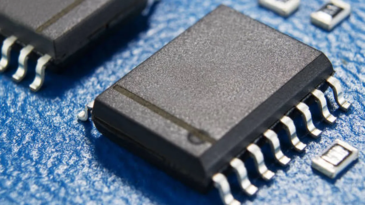
A size such as 5 × 5 mm usually describes an IC package's length and width, while 5 × 5 × 1 mm often adds its height. Those numbers are a useful starting point, but they do not necessarily describe the space occupied by the leads, the distance between terminals, or the PCB pads needed to mount the component.
To interpret IC dimensions, identify what is being measured, which units apply, and how the drawing specifies dimensional limits. This guide explains those distinctions using manufacturer package drawings and clearly labeled illustrative examples. It focuses on mechanical dimensions rather than repeating the background covered in our guide to defining an integrated circuit.
What Do IC Dimension Numbers Mean?
IC dimension numbers describe physical features of the package and its connections. In component listings, they generally refer to the packaged device rather than the silicon die inside it. A datasheet may include several sets of dimensions because engineers need to evaluate different features for placement, assembly, and mechanical clearance.
The main categories are:
- Body size: The length and width of the molded, ceramic, or other package body. Depending on the drawing, small protrusions may be excluded and addressed separately in notes.
- Overall size: The outside dimensions of the package, including projecting leads where applicable. Overall height may be measured from the seating plane rather than from the underside of the body.
- Pitch: The center-to-center spacing between adjacent leads, terminals, or solder balls in the direction indicated.
- Terminal dimensions: Measurements such as lead width, lead length, contact length, or ball diameter.
Length and width describe two perpendicular directions across the package. Height describes its vertical extent, but the reference surfaces matter: body thickness and total seated height are not necessarily the same measurement.
A single IC can therefore have one size for its body, another for its lead-to-lead span, and additional values for its terminals and exposed pad. These are different measurements, not competing descriptions of the same feature. Before comparing two numbers, follow their dimension lines to see where each measurement starts and ends.
How to Read IC Size Numbers
Short size descriptions are convenient for searching a catalog, but they leave out information that a mechanical drawing provides. Start with the column heading or product description, then confirm its meaning in the package outline.
What Does 5 × 5 mm Mean?
When a listing identifies the measurement as body size, 5 × 5 mm usually means a square package body with a nominal length and width of 5 mm. It does not, by itself, specify height, pin count, pitch, exposed-pad dimensions, or a PCB land pattern.
A manufacturer example is Analog Devices' CP-32-7 package drawing. Its title identifies a 32-lead LFCSP with a 5 × 5 mm body. The drawing gives the square body dimension as 4.90 mm minimum, 5.00 mm nominal, and 5.10 mm maximum, and separately identifies a 0.50 mm BSC terminal pitch.
Here, “5 × 5 mm” is a shortened description of a dimension with specified limits. It does not mean every manufactured package measures exactly 5.000 mm on each side. Nor should the CP-32-7 terminal arrangement be assumed to apply to another package simply because both are described as 5 × 5 mm.
What Does 5 × 5 × 1 mm Mean?
As an illustrative catalog entry, 5 × 5 × 1 mm would commonly be read as length × width × height: 5 mm in each horizontal direction and 1 mm vertically. However, that interpretation depends on how the supplier defines its fields.
Check whether the final number represents body thickness, total seated height, a nominal value, or a maximum. Those distinctions matter when a component sits beneath a shield or inside a shallow enclosure.
The CP-32-7 drawing shows why the qualifier matters. Although its title describes a 0.75 mm package height, the side view specifies 0.70 mm minimum, 0.75 mm nominal, and 0.80 mm maximum. A clearance assessment based only on the nominal title value would leave out the permitted variation.
The same approach applies to a rectangular description such as 6.5 × 4.4 × 1.2 mm. This is another illustrative format, not a specification for a particular component. It may mean length × width × height, but manufacturers and distributors do not necessarily present those fields in the same order or use the same measurement boundaries.
For any abbreviated size, check three things: the field labels, the units, and the corresponding mechanical drawing. When both inches and millimeters appear, identify which unit system controls the drawing rather than mixing rounded values from the two columns.
How to Read IC Drawing Symbols
Package drawings often use letters to connect dimension arrows with a table of values. Recognizing common symbols makes a drawing easier to navigate, but the symbol alone is not enough to establish its meaning.
Symbol definitions can vary by manufacturer and package drawing. The following table is a reading aid, not a universal specification.
| Symbol | Common meaning | What to verify in the drawing |
|---|---|---|
| A | Overall package height, often measured from the seating plane | Whether it includes the distance below the body, and whether a maximum is specified |
| A1 | Standoff between the package body and the seating plane | The exact reference surfaces; it is not automatically the assembled solder-joint height |
| D | Package length, commonly body length | Whether the arrows stop at body edges or include other features |
| E | Package width, which may be body width or overall width | Some drawings use E for overall width and E1 for body width; others use different conventions |
| e | Lead, terminal, or ball pitch | The direction of measurement and the centers being referenced |
| L | Lead length or terminal contact length | Whether it describes the contact foot, a projected length, or another defined portion of the lead |
| b | Lead or terminal width; sometimes a ball diameter when paired with a diameter symbol | Where the width is measured and whether the feature is flat or circular |
| D2 / E2 | Often the exposed-pad dimensions on QFN-type packages | Whether these labels actually identify the exposed pad in this drawing |
For example, NXP's SOT96-1 drawing uses E for body width and HE for the span across the leads. It also distinguishes L from Lp, so interpreting both as the same “lead length” would lose information. Texas Instruments' QFN and SON guidance uses D2 and E2 for the exposed-pad dimensions in its package-outline illustration.
Read the relevant views together. The top view helps identify the body outline and orientation; the bottom view reveals terminal and exposed-pad geometry; the side view shows height, standoff, and lead shape. Check the pin-1 indicator when switching between top and bottom views to avoid mirroring the terminal arrangement.
Drawing notes deserve the same attention as the dimension table. They may explain which protrusions are excluded, identify a measurement plane, or define a tolerance that is not repeated beside every dimension. A printed scale or an on-screen ruler is not a substitute for the stated measurements.
What IC Dimension Tolerances Mean
A dimension is more useful when you know its permitted variation. Package drawings may express that variation with plus/minus notation, separate limits, or geometric tolerances associated with basic dimensions.
Understanding ±, MIN, NOM, and MAX
Consider this illustrative dimension:
5.00 ± 0.10 mm
It specifies a range from 4.90 mm to 5.10 mm for the feature being measured, subject to the drawing's conditions and notes. It is not a claim that the feature is exactly 5.00 mm, and it does not describe the statistical distribution of manufactured parts within the limits.
The same limits can be presented in a table:
| MIN | NOM | MAX |
|---|---|---|
| 4.90 mm | 5.00 mm | 5.10 mm |
MIN identifies the lower limit, MAX the upper limit, and NOM the nominal value used to describe the feature. A blank cell is not an instruction to assume zero. If only a maximum is listed, do not invent an equal positive and negative tolerance around it.
For a clearance check, the maximum dimension is usually more relevant than the nominal dimension. Even then, the package limit is only one input: board position, assembly variation, enclosure tolerances, and the chosen mechanical datum can also affect the available clearance.
Understanding TYP, BSC, and REF
These labels serve different purposes and should not be treated as interchangeable ways of saying “approximately.”
| Marking | Meaning | Practical interpretation |
|---|---|---|
| TYP | Typical | Read the drawing's convention. It may describe a representative value or indicate that a callout applies to repeated similar features; it is not, by itself, a minimum or maximum limit. |
| BSC | Basic dimension | A theoretically exact value used to define geometry. Allowable variation is established through the applicable geometric tolerances and drawing requirements, rather than a ± value attached to that basic dimension. |
| REF | Reference dimension | Information provided to help interpret the geometry, generally not an independently toleranced acceptance requirement. |
Microchip's C04-21517 Rev C drawing explicitly defines BSC as a basic dimension with a theoretically exact value shown without tolerances. It defines REF as a reference dimension, usually without tolerance, provided for information.
Thus, 0.50 BSC next to a pitch dimension defines a basic 0.50 mm spacing when the drawing's units are millimeters. It does not mean that actual terminal positions have no manufacturing variation. The relevant positional controls and drawing notes must be read with it.
Analog Devices also uses the expansion “Basic Spacing between Centers” in its BSC glossary. That wording is helpful for understanding pitch, but BSC is not restricted to pin spacing: manufacturers can use basic dimensions for other geometric features.
The distinction is practical. A nominal value describes a size; a basic dimension defines theoretically exact geometry within a tolerancing scheme; a reference dimension supplies supporting information. None should be substituted for another without checking the drawing.
Does IC Size Include the Pins?
Sometimes, but a body-size listing generally does not include leads that project beyond the body. To determine the occupied space, find the overall or lead-tip-to-lead-tip dimensions as well as the body dimensions.
NXP's SOT96-1 SO8 package provides a concrete example. Its official outline specifies:
- Body width, E: 3.8 to 4.0 mm, with 3.9 mm listed as nominal in the package summary.
- Overall lead span, HE: 5.8 to 6.2 mm.
- Lead pitch, e: 1.27 mm.
The midpoint of the stated lead-span limits is 6.0 mm, but that calculated midpoint does not replace the published 5.8–6.2 mm range. A description mentioning a 3.9 mm body width and one mentioning an approximately 6.0 mm lead span can therefore both refer to this package. They measure different features.
This distinction is particularly visible on leaded packages such as SOICs and QFPs. On many leadless packages, the terminals are beneath or near the body edges, making the top-view outline less informative about the connections. For ball-grid packages, the ball arrangement underneath must also be checked. In each case, use the geometry of the selected package rather than assuming that one headline width describes everything.
What Does IC Pin Pitch Mean?
Pin pitch is the center-to-center distance between adjacent pins or terminals in the indicated direction. A 0.50 mm pitch is not a 0.50 mm empty gap between metal edges.
For a simplified illustrative row of equal-width, aligned rectangular terminals, a 0.50 mm pitch and a 0.25 mm terminal width would leave a nominal edge-to-edge gap of 0.25 mm. This subtraction explains the geometry; it is not a minimum-clearance specification. Terminal-width variation, positional tolerances, and the actual shape of the contacts affect the physical gap.
Pitch also differs from pin count. Two packages can have the same number of terminals but different pitches, body dimensions, or terminal arrangements. Conversely, two devices with matching body size and pitch can have different pin assignments or exposed-pad requirements.
IC Dimensions and PCB Footprints
A 5 × 5 mm IC does not necessarily use a 5 × 5 mm PCB footprint. Package dimensions describe the component; a PCB land pattern describes the conductive pads intended to receive it.
Keep these three sets of information separate:
- Package body dimensions describe the enclosure around the internal device.
- Lead or terminal dimensions describe the metal features that connect to the board.
- PCB land-pattern dimensions describe pad sizes, pad positions, and related board-side geometry.
A CAD footprint may contain additional information, including solder-mask openings, paste apertures, a body outline, and a courtyard for placement clearance. These features serve different purposes and do not necessarily share the same outer boundary.
PCB pads are not simply a tracing of the package body. Their dimensions depend on terminal geometry, the intended solder-joint configuration, component and board fabrication tolerances, placement capability, and assembly-process requirements. Exposed-pad packages add another set of dimensions and connection requirements beneath the body.
Texas Instruments' QFN and SON PCB Attachment application note treats package outlines, PCB land patterns, solder-mask design, and stencil design as separate but related subjects. It also notes that application-specific process development is needed; its examples are not a universal footprint recipe.
For practical selection, start with the manufacturer's recommended land pattern for the exact package code, then have the PCB designer or assembly team evaluate it for the intended process. If a CAD library already contains a similarly named footprint, compare its pad geometry and exposed pad against the manufacturer's documentation rather than relying on the name alone.
How to Verify IC Dimensions Before Ordering
Dimensional verification is most useful when it is tied to a specific orderable part number. A family name or a product photograph may help narrow the search, but neither establishes the exact package variant.
Before placing an order, confirm the following:
| Item to verify | What to compare |
|---|---|
| Exact manufacturer part number | The full ordering code on the quotation, bill of materials, and manufacturer documentation |
| Package suffix or package code | The manufacturer's ordering-information table and the corresponding package outline |
| Body dimensions | Length, width, height, and the stated limits rather than only a catalog summary |
| Pin or terminal count | The connection arrangement and how any exposed pad is identified |
| Pitch | Center-to-center spacing in the relevant direction or directions |
| Manufacturer package drawing | The correct outline, variant, drawing identifier, and applicable notes |
| Recommended land pattern | Board-side pad geometry, exposed-pad treatment, and relevant assembly guidance |
| Datasheet revision | The document version used for engineering approval, together with the package-drawing revision |
Different suffixes within an IC family may identify different packages. Other suffixes can indicate temperature grade, qualification, packing format, or another ordering attribute. Decode them using the manufacturer's ordering information instead of assuming that every suffix change has the same meaning.
If an alternative component is proposed, compare both its mechanical and electrical requirements. Matching length, width, and pin count does not establish pin compatibility, equivalent performance, or suitability for an existing footprint. Likewise, dimensional agreement alone is not evidence of authenticity or complete manufacturer traceability.
When sourcing ICs, dimensional verification should be performed together with the exact manufacturer part number, package code, and datasheet revision. Vigorcomp, operated by VIGOR COMPONENTS PTE LTD, is an independent electronic components distributor based in Singapore, supporting customers worldwide with sourcing for active, obsolete, hard-to-find, and long lead-time components. This business description is set out in the company's official FAQ.
When submitting an inquiry, include the complete part number and any package restrictions that affect acceptance. Availability, product condition, traceability requirements, and any requested inspection or testing should be discussed separately from mechanical fit.
IC dimension numbers become easier to use when each is tied to a specific feature: body size for the enclosure, overall dimensions for the component's extent, pitch for terminal spacing, and a land pattern for its board connections. The package drawing brings those measurements together; the complete ordering code identifies which drawing belongs to the part you intend to buy.