
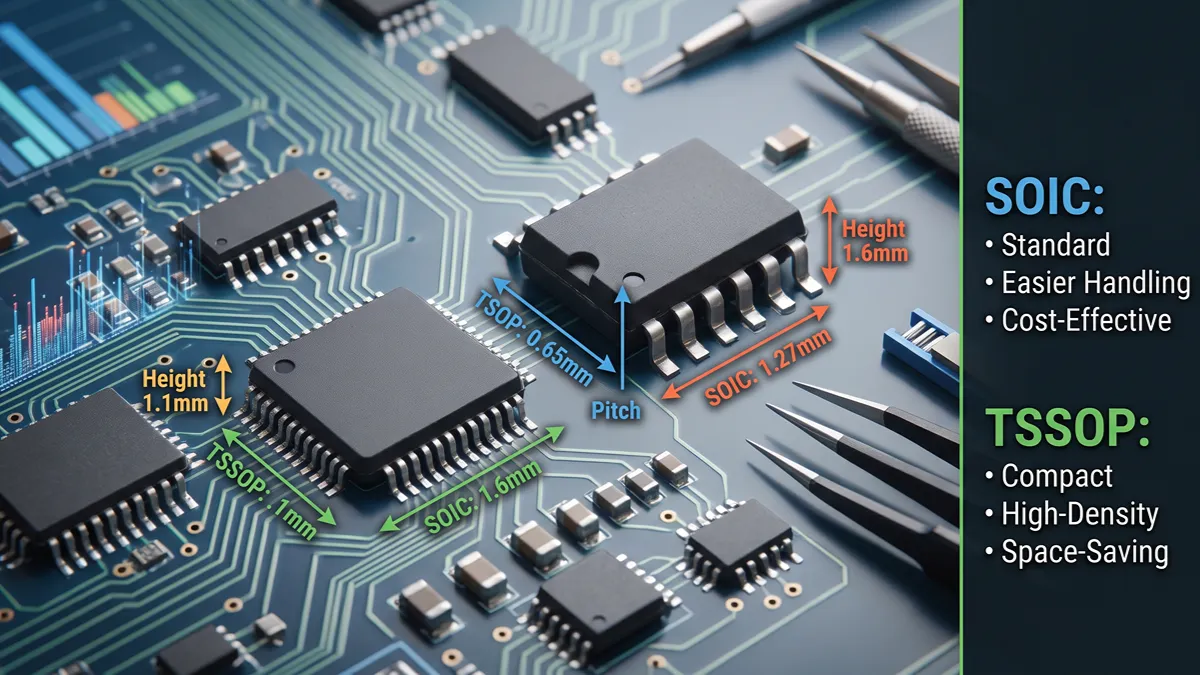
Both TSSOP and SOIC are surface-mounted IC packages with gull-wing leads, and at a glance they look like close cousins. They are not. The differences between them, in lead pitch, body size, height, routing difficulty, and assembly tolerance, are large enough to shape PCB layout decisions, manufacturing yield, and even how easily you can debug a prototype.
The core trade-off is straightforward. TSSOP shrinks the footprint and lowers the profile, which helps when board area is tight or component density is high. SOIC spreads the leads farther apart, which makes routing, soldering, inspection, and rework noticeably easier. Neither package is universally better. A battery-powered handheld may need every square millimeter TSSOP saves, while a low-volume industrial board built for field serviceability may be better served by SOIC's forgiving geometry.
For most designers, the choice between TSSOP and SOIC comes down to board space versus manufacturability.
TSSOP vs SOIC
| Feature | TSSOP | SOIC |
|---|---|---|
| Full name | Thin Shrink Small Outline Package | Small Outline Integrated Circuit |
| Typical lead pitch | 0.5 mm or 0.65 mm | 1.27 mm |
| Package height | Lower (typically 0.85–1.0 mm) | Higher (typically 1.38–1.75 mm) |
| PCB footprint | Smaller | Larger |
| Pin density | Higher | Lower |
| PCB routing | More demanding | Easier |
| Hand soldering | More difficult | Easier |
| Rework | More difficult | Easier |
| Assembly tolerance | Tighter | More forgiving |
| Typical use | Compact, high-density designs | Prototypes, industrial and general-purpose designs |
The table tells most of the story. TSSOP packs the same pin count into a smaller body with finer lead spacing, and it does so with a thinner profile. SOIC trades that density for a wider process window — leads you can see without a microscope, pads you can route without narrowing traces to absurd widths, and solder joints you can inspect and rework with basic tools.
Choose TSSOP when space matters most; choose SOIC when assembly simplicity and serviceability matter more.
Size, Pitch, and PCB Footprint
Package Size and Height
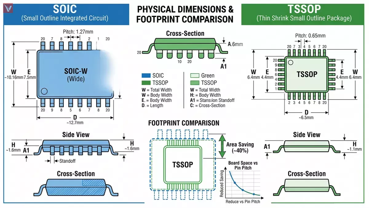
The names encode geometry. "Thin" means the package sits lower above the board. Typically 0.85 to 1.0 mm for TSSOP versus 1.38 to 1.75 mm for SOIC. "Shrink" means the body is narrower and shorter for the same pin count, achieved by reducing the lead pitch.
A concrete comparison makes this visible. Toshiba's SOIC-16 measures 6.0 mm wide × 10.2 mm long with a 1.38 mm profile. The same manufacturer's TSSOP-16 measures 5.4 mm wide × 6.4 mm long with a 1.0 mm profile. The footprint drops from roughly 61 mm² to about 35 mm² — a 43% reduction — and the package stands 0.38 mm shorter. On a dense board with a dozen such parts, that adds up fast.
Exact dimensions vary by manufacturer and package sub-family, and SOIC itself comes in narrow-body and wide-body variants under different JEDEC designations (MS-012 for narrow, MS-013 for wide). The mechanical drawing in the component datasheet is always the final authority.
Lead Pitch
SOIC uses a 1.27 mm lead pitch across virtually all variants — a figure rooted in the JEDEC MS-012 standard. TSSOP most commonly uses 0.65 mm, though 0.5 mm appears on higher-pin-count versions.
Pitch determines how wide your routing channels can be between pads, how much solder paste the stencil deposits per pad, how much placement error the pick-and-place machine can tolerate, and how likely adjacent leads are to bridge during reflow. At 1.27 mm, there is enough room between pads for a respectable trace and a solder mask dam that holds. At 0.65 mm, you are routing between pads that are barely half a millimeter apart, and solder paste control becomes the dominant process variable.
PCB Space Savings
TSSOP saves board area through two mechanisms working simultaneously: a smaller package body and tighter lead spacing. The body shrink reduces the area the part physically occupies. The pitch shrink narrows the strip of board consumed by the fan-out region — the space where leads emerge from the package and connect to traces. A same-pin-count footprint comparison between SOIC-16 and TSSOP-16 shows that the savings come from both the outline and the land pattern, not just the package height.
Soldering, PCB Assembly, and Rework
Hand Soldering
SOIC is the package most engineers learn to hand-solder first, and for good reason. The 1.27 mm pitch leaves enough room between adjacent leads for a standard soldering iron tip, visual inspection is possible without magnification, and solder bridges — when they happen — are obvious and easy to fix with a bit of wick.
TSSOP can be hand-soldered, but it demands more technique. The 0.65 mm pitch means leads sit close enough that a conventional chisel tip will bridge two pads at once. Most engineers working with TSSOP turn to drag soldering with a fine tip and generous flux, or use a hot-air station. It is not prohibitively difficult, but it punishes sloppy flux application and rewards practice.
Reflow Assembly
Both packages are mature, widely supported options for automated SMT production. The difference is process sensitivity.
TSSOP's tighter pitch means the stencil aperture design matters more. Solder paste deposition per pad is smaller in volume, so variation in paste height or aperture alignment has a proportionally larger effect on the joint. Placement accuracy tolerances are tighter, and reflow profiles need to be controlled more carefully to avoid tombstoning or insufficient wetting. None of this is exotic — any competent SMT line handles TSSOP routinely — but the process window is narrower.
SOIC's 1.27 mm pitch gives you a wider margin. Larger pads accept more paste, bridging is less likely, and placement machines with moderate accuracy are sufficient. For lines running mixed product families with varying complexity, SOIC is the lower-risk option.
Inspection and Rework
Visual inspection tracks the same pattern. SOIC solder joints are large enough to check under a bench microscope or even with good lighting and a magnifier. Probing a pin during debugging is straightforward — the lead is accessible, and the pad has room for a probe tip.
TSSOP joints are smaller and closer together. AOI (automated optical inspection) handles both well in production, but manual inspection and rework are harder. Desoldering a single TSSOP lead without disturbing its neighbors requires finer tools and steadier hands. For boards that will see repeated prototyping cycles or field repair, this matters.
Thermal Performance and Reliability
Package size alone does not determine how well a part sheds heat. A smaller body can actually make thermal management harder if it means less copper area connected to the leads or a smaller exposed pad — but the relationship is not always that simple.
Thermal resistance values (θJA, θJC) depend on leadframe construction, package geometry, the presence and size of an exposed thermal pad, the copper pours connected to that pad, and the PCB layer stackup. Two packages from the same manufacturer carrying the same die can report meaningfully different θJA numbers. The only reliable way to compare is to open both datasheets and read the thermal table — including the footnotes that specify the test board conditions.
Some TSSOP variants include an exposed pad on the underside that solders to a copper pour on the PCB, dramatically lowering thermal resistance. Some SOIC variants do the same. A TSSOP with a well-designed exposed pad can outperform a SOIC without one, and vice versa. Check the datasheet for θJA, θJC, maximum junction temperature, power dissipation limits, exposed-pad requirements, and recommended PCB copper area before drawing conclusions.
On reliability: SOIC tends to survive repeated prototype handling, probing, and rework cycles better, simply because its leads and pads are larger and more robust to mechanical stress. TSSOP is equally reliable in volume production when the PCB layout and SMT process are well controlled. The difference shows up on the workbench, not on the assembly line.
Package size alone is not a reliable indicator of thermal performance.
Cost and Manufacturing Trade-Offs
Component price depends on the IC manufacturer, device family, production volume, distributor inventory, and market demand for that specific part number. A particular IC offered in both packages may carry the same unit price, a small premium for TSSOP, or occasionally a premium for SOIC if the TSSOP version is higher volume.
TSSOP reduces PCB area, which can lower board cost in space-constrained products, or matter not at all on a board with unused space. Finer routing rules for TSSOP may require more layers in dense designs, which raises board cost. Tighter assembly tolerances may not increase per-unit assembly price at a modern SMT line, but they can affect yield during process setup or when switching between product runs.
SOIC's larger geometry makes the assembly process more forgiving, which translates to fewer setup headaches in low-volume or mixed-product manufacturing. Easier rework has real economic value in prototyping and low-volume production, where a discarded board costs more than the few minutes spent fixing a solder bridge.
Can You Replace SOIC With TSSOP?
Usually, not without changing the PCB footprint.
The same IC is often available in both SOIC and TSSOP versions with identical electrical function and logical pinout. That does not make the packages interchangeable. The lead pitch differs (1.27 mm versus 0.65 mm), the body dimensions differ, the recommended land pattern differs, the package height differs, and the thermal characteristics may differ if one variant has an exposed pad and the other does not.
An SOIC-8 and a TSSOP-8 may share the same eight electrical pins in the same logical order, but their physical footprints are completely different. Dropping a TSSOP-8 onto a board laid out for SOIC-8 will not work — the pads will not align, and no amount of creative soldering will bridge a 0.65 mm pitch part onto 1.27 mm pads.
Before specifying an alternate package — whether for design flexibility or sourcing substitution — verify the package code, mechanical drawing, pinout, recommended land pattern, thermal data, and assembly requirements in the datasheet. Sourcing teams considering a TSSOP alternate for a SOIC design should treat it as a PCB change, not a drop-in substitution.
An SOIC-8 and a TSSOP-8 may have the same eight electrical pins but completely different PCB footprints.
Which Package Should You Choose?
| Design Priority | Better Starting Point |
|---|---|
| Smallest PCB footprint | TSSOP |
| Low package height | TSSOP |
| High component density | TSSOP |
| Easy hand soldering | SOIC |
| Easy PCB routing | SOIC |
| Easy inspection and rework | SOIC |
| Simple prototyping | SOIC |
| High-volume SMT production | Either, depending on process |
| Higher-power IC | Check the datasheet |
This table is a starting point, not a decision engine. Real selection involves weighing several factors simultaneously.
When TSSOP makes sense. If the product is space-constrained, a wearable, a handheld instrument, a densely packed mobile device. And the footprint and height savings are the primary value. TSSOP also fits naturally on boards already designed for fine-pitch SMT assembly, where the pick-and-place, stencil, and reflow processes are already configured for 0.5 mm or 0.65 mm pitch components. In high-volume consumer electronics, the PCB area savings compound across the board and can justify the tighter process control.
When SOIC makes sense. Prototypes and low-volume boards benefit from everything SOIC's wider pitch provides: easier routing, easier hand soldering, easier probing during debug, easier inspection, and easier rework when something goes wrong. Industrial equipment designed for long service life and field repair is another natural fit — a technician with a soldering iron and a multimeter can service a SOIC board without specialized microsoldering tools. Boards with generous area budgets and no height constraints gain little from TSSOP's shrink.
When neither is obviously right. High-volume production with an established SMT line can handle either package efficiently, so the decision may come down to component availability and thermal performance. For higher-power ICs, the package with the lower θJA, which could be either one, depending on exposed-pad design, wins regardless of footprint.
If both packages are available for the same IC, start by comparing board-space requirements, assembly capability, and thermal performance — not just package dimensions.
Frequently Asked Questions
Is TSSOP smaller than SOIC?
Yes. For the same pin count, TSSOP generally has a smaller body footprint, lower package height, and tighter lead pitch than SOIC. A TSSOP-16 typically occupies roughly 40–45% less board area than a SOIC-16.
Which is easier to solder, TSSOP or SOIC?
SOIC is easier to solder by hand. Its 1.27 mm lead pitch provides enough space between pads for a standard iron tip and makes solder bridges easier to see and fix. TSSOP can be hand-soldered with the drag-soldering technique and good flux, but it is less forgiving.
Can TSSOP and SOIC use the same PCB footprint?
No. Their lead pitch, body dimensions, and recommended land patterns are all different. A PCB designed for SOIC cannot accept a TSSOP part and vice versa without a layout change.
Is SOIC better for prototyping?
SOIC is often preferred for prototypes because it is easier to route, solder, probe, inspect, and rework. For boards that will go through multiple revision cycles or manual debugging, these practical advantages matter.
Does TSSOP have worse thermal performance than SOIC?
Not necessarily. Thermal performance depends on the specific component's leadframe design, exposed pad, package geometry, and PCB layout. Compare θJA, θJC, power dissipation limits, and the manufacturer's PCB copper recommendations in the datasheet rather than relying on package type alone.