
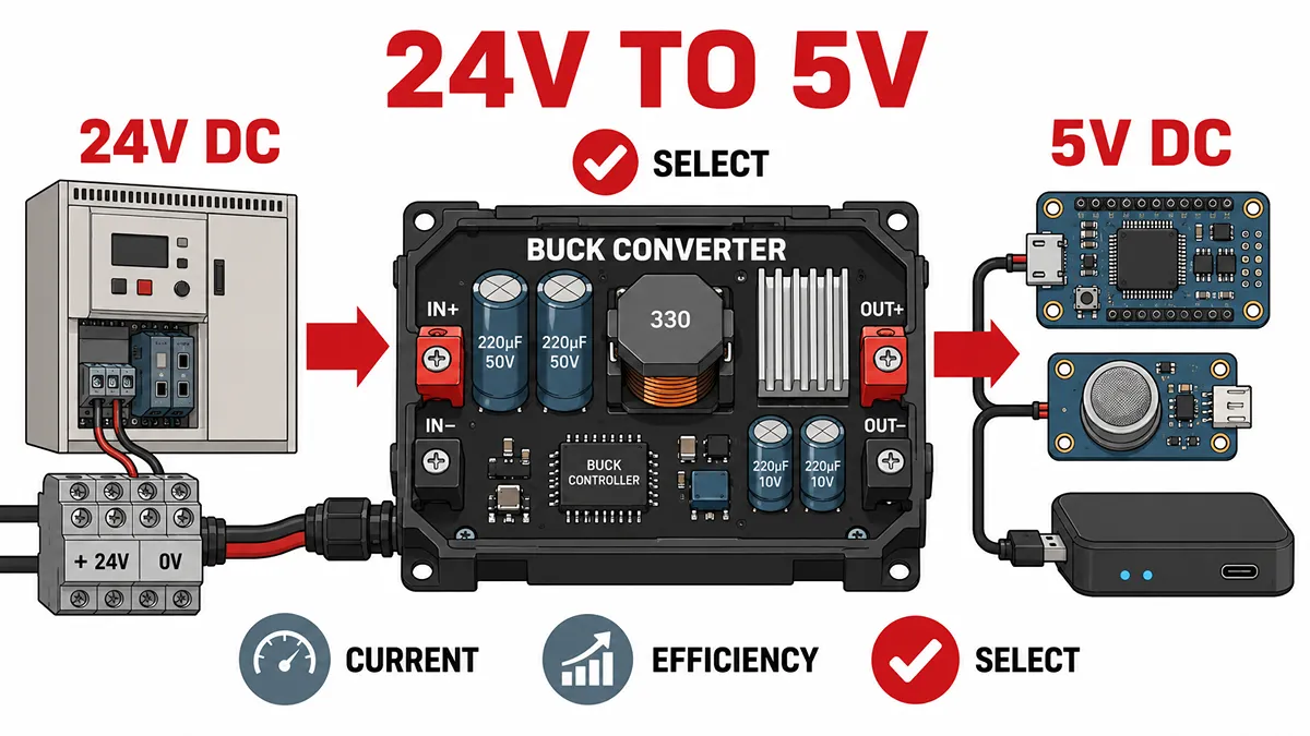
Converting a 24V DC bus to a regulated 5V rail is common in industrial controllers, embedded systems, networking equipment, and other electronic assemblies. A successful design requires more than selecting a device with a 5V output: engineers must define the actual input-voltage range, load current, thermal limits, transient conditions, protection strategy, and PCB layout requirements.
For low-current applications, a linear regulator may be acceptable. However, when the input-to-output voltage difference is large and the 5V load current is more than a few tens of milliamps, a switching buck converter is usually the more practical solution because it greatly reduces power loss and heat generation.
Define the Input, Output, and Protection Requirements
Before choosing a 24V to 5V converter, define the electrical and environmental conditions of the final application. “24V” is often a nominal value rather than the highest voltage the converter will encounter.
| Parameter | Questions to Define | Why It Matters |
|---|---|---|
| Input voltage range | What are the minimum, normal, and maximum steady-state input voltages? | The converter must operate across the complete normal input range. |
| Input transients | Are there switching surges, inductive load transients, reverse-polarity risks, or other abnormal conditions? | The IC voltage rating and protection circuit must tolerate the highest voltage that can reach the converter. |
| Output voltage | Is the rail fixed at 5V, and what tolerance is required? | Logic circuits, sensors, and communication modules may have different supply-voltage limits. |
| Output current | What are the continuous, startup, and peak load currents? | The converter, inductor, diode or MOSFETs, and output capacitors must support the highest expected current. |
| Ripple and noise | How much output ripple can the load tolerate? | Ripple requirements influence switching frequency, inductor value, output capacitance, and layout. |
| Ambient temperature | What temperature range will the PCB operate in? | Higher ambient temperature reduces the available thermal margin. |
| Protection requirements | Are TVS diodes, fuses, eFuses, reverse-polarity protection, or input filters required? | Protection components determine the voltage and current stress seen by the converter. |
A DC-DC converter is the general term for a circuit that converts one DC voltage level to another. A 24V-to-5V design can use either a linear regulator or a switching regulator. For most mediumand high-current applications, a step-down switching regulator, also called a buck converter, is preferred.
If your application requires a 12V rail instead of 5V, see our Ultimate Guide to Selecting a 24V to 12V DC Converter for the same 24V bus.
Can a Linear Regulator Convert 24V to 5V?
Yes, a linear regulator can reduce 24V to 5V if its input-voltage rating, output-current capability, and thermal limits are suitable. The main limitation is power dissipation.
For a linear regulator, the approximate power dissipated in the device is: \(P_D = (V{IN} - V{OUT}) \times I_{OUT}\) Where:
- \(P_D\) is the power dissipated by the regulator in watts
- \(V_{IN}\) is the regulator input voltage
- \(V_{OUT}\) is the regulated output voltage
- \(I_{OUT}\) is the output current
For a 24V input, 5V output, and 1A load: \(P_D = (24V - 5V) \times 1A = 19W\) The regulator must therefore dissipate approximately 19W as heat. This makes a conventional linear regulator impractical for most 1A applications unless a substantial thermal solution is used.
The estimated junction temperature is: \(T_J = T_A + P_D \times R_{\theta JA}\) Where:
- \(T_J\) is the junction temperature
- \(T_A\) is the ambient temperature
- \(R_{\theta JA}\) is the junction-to-ambient thermal resistance for the specific package and PCB layout
For example, if a device dissipates 19W at a 25°C ambient temperature and the effective thermal resistance is 65°C/W, the simplified estimate would be: \(T_J = 25^\circ C + (19W \times 65^\circ C/W) = 1260^\circ C\) This number is not an achievable operating temperature. It shows that the thermal requirement is far beyond the safe operating range of a typical regulator; in practice, the device may enter thermal shutdown, current limiting, or fail if protection is inadequate. The actual thermal result depends on the specific package, copper area, airflow, heatsink design, and the device’s thermal-protection behavior. TI’s linear-regulator guidance similarly calculates dissipation from the input-output voltage difference and load current, then evaluates allowable dissipation against junction temperature and thermal resistance.
When Is a Linear Regulator Acceptable?
A linear regulator may still be appropriate when:
- The output current is very low
- The input-to-output voltage difference is small
- Low noise is more important than conversion efficiency
- The design has sufficient thermal margin
- A buck converter creates unnecessary cost or complexity for the application
For example, at 24V input, 5V output, and 50mA load: \(P_D = (24V - 5V) \times 0.05A = 0.95W\) Even 0.95W can require thermal review, especially in a compact enclosure or at high ambient temperature. Always verify the regulator’s input rating, maximum junction temperature, package thermal data, and recommended PCB copper area in the manufacturer's datasheet.
Select a 24V to 5V Buck Converter
A buck converter converts a higher DC input voltage to a lower regulated output voltage by switching energy through an inductor. Compared with a linear regulator, it can achieve much higher efficiency because the voltage difference is not continuously dissipated as heat in the regulating element.
For a 24V-to-5V design, select the right power supplies and board mount DC-DC converters based on the actual electrical conditions rather than the nominal bus voltage alone.
Select the Correct Input-Voltage Rating
Start with the highest voltage that can reach the converter input after any TVS diode, fuse, reverse-polarity circuit, or input filter.
Do not select an IC only because its maximum input rating is slightly above 24V. A nominal 24V rail may have normal tolerance, startup variation, switching transients, or application-specific surge conditions. The converter’s absolute maximum input-voltage rating must remain above the highest protected input voltage, with appropriate engineering margin.
For example, a 60V-rated buck converter may be suitable for a design where the protected input voltage can exceed 36V or 40V, but the correct choice depends on the real input specification and protection clamp voltage. TI’s LM76003 is one example of a synchronous buck regulator specified for a 3.5V to 60V operating input range and up to 3.5A output current; it is an example only, not a universal recommendation for every 24V-to-5V design.
Define Continuous and Peak Output Current
Choose a converter with sufficient current capability for:
- Continuous 5V load current
- Startup current
- Capacitive inrush current
- Short-duration peak load
- Thermal derating at the highest ambient temperature
Do not select a converter solely by its headline current rating. Check the datasheet for switching-current limit, thermal derating, output-current capability across input voltage, switching frequency, and PCB conditions.
Choose Synchronous VS Non-Synchronous Rectification
A non-synchronous buck converter uses a diode as the freewheeling path. This approach can be simple and cost-effective, especially at lower output currents.
A synchronous buck converter replaces the diode with a controlled low-side MOSFET. This can reduce conduction loss, particularly when output current is higher or output voltage is low. The actual efficiency improvement depends on the load current, MOSFET resistance, switching frequency, diode voltage drop, and control method.
For a 24V-to-5V converter, synchronous rectification is often worth considering when:
- The 5V rail supplies moderate or high current
- Board temperature is a key concern
- Higher efficiency is required
- The application has limited PCB area for thermal spreading
Select Switching Frequency and Inductor Value
Higher switching frequency can reduce the required inductance and allow smaller magnetic components. It may also increase switching loss and place greater demands on PCB layout and EMI control.
Lower switching frequency can reduce switching loss in some designs, but it generally requires a larger inductor and may increase output ripple or transient-response tradeoffs. The best frequency depends on the converter IC, load profile, efficiency target, EMI limits, available board area, and thermal requirements.
For a buck converter operating in continuous-conduction mode, a simplified starting equation for inductor selection is: \(L = \frac{V_{OUT} \times (V_{IN} - V_{OUT})}{V_{IN} \times f_{SW} \times \Delta I_L}\) Where: \(L\) is the inductance \(V_{IN}\) is the input voltage \(V_{OUT}\) is the output voltage \(f_{SW}\) is the switching frequency \(\Delta I_L\) is the selected peak-to-peak inductor ripple current
A common starting point is to set inductor ripple current as a portion of the maximum output current, then verify the result against the IC datasheet, transient-response target, inductor saturation current, RMS current rating, and efficiency goal.
The inductor saturation-current rating must exceed the highest expected peak inductor current. The inductor RMS-current rating must also support the expected operating current without excessive temperature rise.
Design the 24V to 5V Buck Converter PCB Layout
A correct schematic does not guarantee a reliable switching power supply. PCB layout strongly affects converter efficiency, EMI, output ripple, thermal performance, and stability.
Place the Input Capacitor First
Place the high-frequency input ceramic capacitor as close as possible to the buck converter’s VIN and power-ground pins. This capacitor supplies the high di/dt switching current locally and helps minimize the input switching loop.
Keep the loop formed by the input capacitor, high-side switch, low-side switch or freewheeling diode, and ground return as small as possible. A compact loop reduces parasitic inductance, ringing, and radiated EMI. TI’s step-down-converter layout guidance identifies input-capacitor placement as the first layout priority and recommends routing it directly to the IC with minimal connection inductance.
Control the Switching Node
The SW node changes voltage rapidly and can couple noise into nearby traces. Keep the switching-node copper area only as large as needed for current handling and component connection.
Avoid routing sensitive feedback, enable, compensation, communication, or analog-signal traces near the SW node. Keep the feedback network away from noisy power paths and route it according to the IC manufacturer’s recommended layout.
Build a Clean Ground Return Path
Use a continuous ground plane where possible. Connect the power ground, input-capacitor ground, output-capacitor ground, and IC ground according to the manufacturer’s recommended layout, not by arbitrary routing.
The feedback ground and sensitive analog ground connections should avoid sharing a noisy high-current return path. A poor ground return can increase ripple, create unstable regulation, or worsen EMI performance.
Use Copper and Thermal Vias Correctly
If the regulator IC includes an exposed thermal pad, follow the datasheet’s recommended land pattern and thermal-via arrangement. The exposed pad usually connects to a copper region that transfers heat into internal or bottom PCB layers.
Thermal vias can improve vertical heat flow, but their diameter, quantity, pitch, tenting, filling, and solder-mask treatment should match the IC manufacturer’s recommendation and the PCB fabricator’s process capability. Do not assume one via size is correct for every package or assembly process.
Use sufficient copper area on the recommended layers to spread heat from the IC, inductor, diode, and other high-loss components. Then verify the temperature rise on the actual PCB at maximum input voltage, maximum load current, and worst-case ambient temperature.
Verify the Design Before Production
Before releasing the design, verify the converter under realistic electrical and thermal conditions.
- Test at minimum, nominal, and maximum input voltage
- Test at no load, normal load, peak load, and startup load
- Measure 5V output ripple and transient response
- Check inductor and IC temperature at the highest expected ambient temperature
- Verify startup behavior and protection response
- Measure conducted and radiated EMI when the product requires compliance testing
- Confirm that the selected components meet voltage, current, temperature, and lifecycle requirements
A 24V-to-5V buck converter is not fully validated until the complete design—IC, inductor, capacitors, protection network, PCB layout, enclosure, and load—is tested together.
Component Sourcing Checklist
For production designs, component sourcing should preserve the electrical and thermal assumptions used during engineering validation.
When purchasing the buck converter IC, inductor, capacitors, TVS diode, and related components, confirm:
- Exact manufacturer part number and package
- Input-voltage and output-current ratings
- Temperature grade and qualification requirements
- Datasheet revision and lifecycle status
- Approved alternate parts, if required
- Date-code, traceability, and quality-control requirements
- Availability for prototype, pilot, and production quantities
Vigor Components can support BOM sourcing for power-management components and help identify available parts or alternatives based on the required electrical specifications.