
Introduction to the STM32F103C8T6 ADC
The STM32F103C8T6 microcontroller, built around the ARM Cortex-M3 core, is highly regarded for its balance of processing speed and versatile peripheral integration. Among its most critical features is its analog-to-digital converter (ADC) architecture. This MCU features two 12-bit ADCs that operate independently or in dual mode, allowing hardware engineers to capture highly accurate analog signals from the physical environment.
With a rapid conversion time of just 1 µs (achieved at the shortest 1.5 + 12.5 cycles) at a 14 MHz ADC clock, the STM32F103C8T6 is more than capable of handling high-frequency sensor data. Note that the ADC clock (derived from APB2) must not exceed 14 MHz for reliable operation. This level of performance is essential for industrial automation, medical monitoring equipment, and precise motor control systems. In these demanding applications, engineers rely heavily on the 12-bit resolution to detect minute voltage changes, resolving analog signals into 4,096 discrete digital steps.
However, achieving this theoretical precision in a real-world printed circuit board (PCB) requires more than just calling a software function. It demands a deep understanding of pin configurations, memory access strategies, and hardware-level noise reduction. Furthermore, the integrity of the ADC readings is heavily dependent on the authenticity of the silicon itself, underscoring the importance of sourcing original components for production builds.
STM32F103C8T6 ADC Pinout and Channels
To begin sampling analog data, you must first understand how the internal ADC is mapped to the physical pins of the microcontroller. The STM32F103 series supports up to 16 external analog channels. However, because the STM32F103C8T6 utilizes the smaller 48-pin LQFP package, only 10 of these external channels are physically accessible to the designer.
When designing your schematic, it is crucial to route your analog sensor traces to the correct GPIO pins. The pins dedicated to ADC input are located on Port A and Port B.
Below is the specific pinout mapping for the external ADC channels on the STM32F103C8T6:
| ADC Channel | Physical Pin (LQFP48) | GPIO Port | Typical Use Case |
|---|---|---|---|
| ADC12_IN0 | Pin 10 | PA0 | General analog sensor input |
| ADC12_IN1 | Pin 11 | PA1 | General analog sensor input |
| ADC12_IN2 | Pin 12 | PA2 | General analog sensor input |
| ADC12_IN3 | Pin 13 | PA3 | General analog sensor input |
| ADC12_IN4 | Pin 14 | PA4 | General analog sensor input |
| ADC12_IN5 | Pin 15 | PA5 | General analog sensor input |
| ADC12_IN6 | Pin 16 | PA6 | General analog sensor input |
| ADC12_IN7 | Pin 17 | PA7 | General analog sensor input |
| ADC12_IN8 | Pin 26 | PB0 | Often used for current sensing |
| ADC12_IN9 | Pin 27 | PB1 | Often used for voltage monitoring |
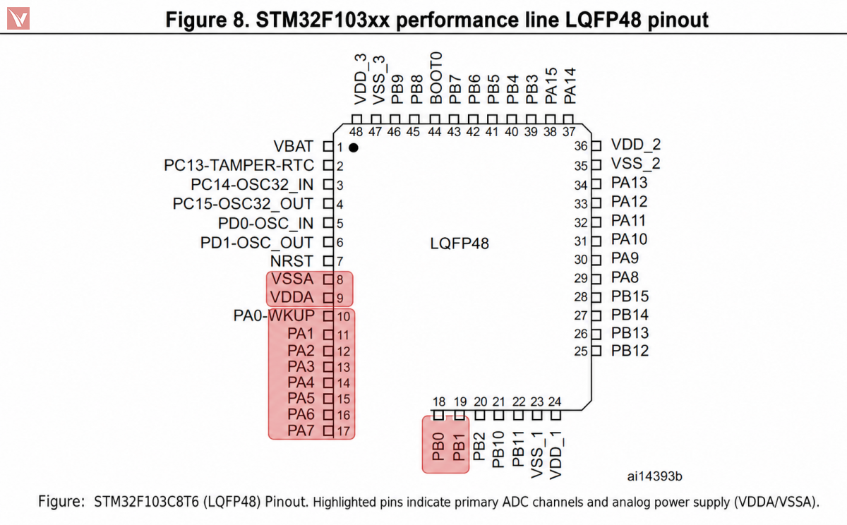
Note that on the 48-pin package, the analog reference voltage pin (VREF+) is internally tied to the analog power supply pin (VDDA). This means your ADC reference voltage will always be equal to your VDDA supply, which is typically 3.3V.
Polling vs. Interrupt vs. DMA: Which to Choose?
Once your hardware is wired, you must decide how the ARM Cortex-M3 processor will retrieve the converted digital values from the ADC data register. The STM32 architecture offers three distinct methods for this task. Selecting the right method is critical for maintaining system stability and preventing processor bottlenecks.
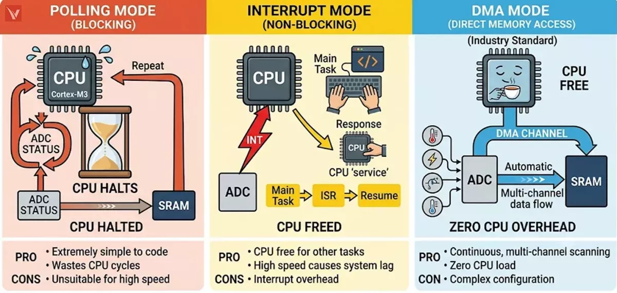
Polling Mode (Blocking): The CPU starts the conversion and halts all other operations while waiting in a loop for the ADC to finish.
- Pros: Extremely simple to write and debug.
- Cons: Waste valuable CPU cycles. Unsuitable for time-critical industrial systems or multi-channel sampling.
Interrupt Mode (Non-Blocking): The ADC triggers a hardware interrupt once a conversion is complete, prompting the CPU to briefly pause its current task, read the register, and return.
- Pros: Frees up the CPU to perform other tasks while the ADC works in the background.
- Cons: At high sampling rates (e.g., 1 MHz), constant interrupt requests will significantly consume CPU cycles, potentially impacting other time-critical tasks.
DMA Mode (Direct Memory Access): The ADC bypasses the CPU entirely. Upon completing a conversion, the hardware DMA controller automatically moves the data from the ADC register directly into the system SRAM.
- Pros: Zero CPU overhead. Ideal for continuous, multi-channel scanning.
- Cons: Requires a slightly more complex initial software configuration.
For professional embedded systems—especially those reading multiple sensors simultaneously—DMA is the absolute industry standard. It ensures deterministic timing and leaves the Cortex-M3 free to run complex filtering algorithms or communication protocols.
How to Configure ADC with DMA in STM32CubeIDE
Setting up the ADC with DMA might sound intimidating, but STM32CubeIDE's graphical configuration tool simplifies the process significantly. Follow these steps to configure a continuous, non-blocking multi-channel ADC read.
1. Enable the ADC Channels:
- Open your .ioc device configuration file.
- Navigate to Analog > ADC1.
- Check the boxes for the input channels you intend to use (e.g., IN0 and IN1).
2. Configure ADC Parameters:
- In the Parameter Settings pane, set Scan Conversion Mode to Enable. This allows the ADC to read multiple channels in a sequence.
- Set Continuous Conversion Mode to Enable so the ADC automatically restarts the sequence after finishing.
- Adjust the Number of Conversion to match your active channel count.
- Set the Sampling Time for each rank. Higher sampling times (e.g., 71.5 or 239.5 cycles) yield more stable and accurate readings for high-impedance sensors.
3. Add the DMA Request:
- Switch to the DMA Settings tab within the ADC1 configuration.
- Click Add and select ADC1.
- Change the Mode from Normal to Circular. This tells the DMA to wrap around to the beginning of your memory buffer automatically.
- Ensure the Data Width is set to Half Word (16 bits) for both Peripheral and Memory, perfectly accommodating the 12-bit ADC output.
4. Generate and Write Code:
- Save the file to generate the C code.
- In your \(main.c\) , create a 16-bit array to hold the data: \(uint16_t adc_buffer[2]\) ;
- Start the DMA process before your main while(1) loop by calling:
\(HAL_ADC_Start_DMA(&hadc1, (uint32_t*)adc_buffer, 2)\) ;
To convert the raw 12-bit ADC value (0-4095) into a real voltage, apply this formula in your code: float voltage = adc_buffer[0] * (VDDA / 4095.0f); // VDDA is typically 3.3V
Your adc_buffer array will now continuously and automatically update with the latest sensor values, requiring no further intervention from the CPU.
Reading the Internal Temperature Sensor
Beyond external pins, the STM32F103C8T6 includes an internal temperature sensor connected internally to ADC1_IN16. This is a highly practical feature for monitoring the thermal state of your PCB or executing temperature compensation for other sensitive components.
To utilize this feature, simply enable the "Temperature Sensor Channel" in the STM32CubeIDE ADC settings. The ADC will read an analog voltage that changes linearly with the die temperature.
To convert this raw 12-bit value into a meaningful Celsius reading, you must apply the formula provided in the STMicroelectronics datasheet: \(temperature = ((V25 - V_sense) / Avg_Slope) + 25.0
V25 = 1.43 V (typ.)
Avg_Slope = 4.3 mV/°C (typ.) = 0.0043 V/°C\) 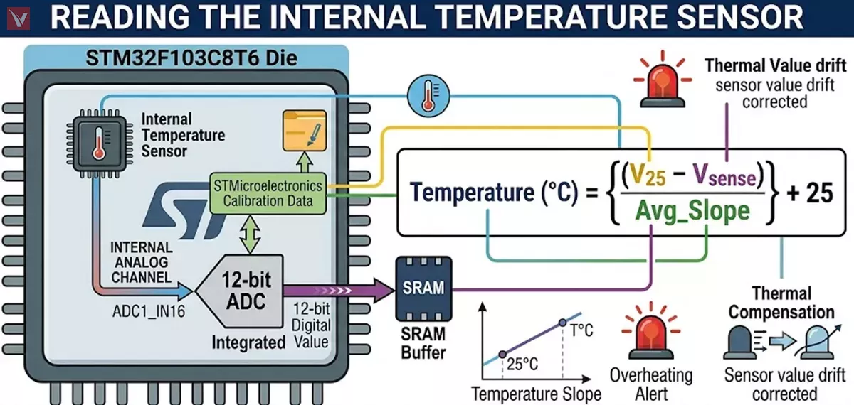
- V25: The voltage value at 25°C (typically 1.43V).
- Avg_Slope: The rate of voltage change per degree Celsius (typically 4.3 mV/°C).
- V_sense: The actual voltage you calculated from the ADC reading.
Keep in mind that this internal sensor is best suited for detecting significant thermal variations (like overheating) rather than highly precise ambient room temperature measurements.
Hardware Tips to Reduce ADC Noise
Firmware configuration is only half the battle. A 12-bit ADC is sensitive enough to pick up microscopic voltage ripples caused by digital switching, power supply instability, and poor PCB layout. If your ADC readings are fluctuating wildly, software averaging alone will not fix a fundamentally noisy hardware design.
To achieve true high-precision sampling, implement the following hardware strategies:
- Isolate the Analog Supply (VDDA): Never connect VDDA directly to the noisy digital VDD line without filtering. Use a ferrite bead and decoupling capacitors to create a low-pass LC filter between VDD and VDDA.
- Strategic Decoupling: Place a 1 µF ceramic capacitor in parallel with a 10 nF ceramic capacitor as close to the VDDA and VSSA pins as physically possible.
- Ground Planes: Use a solid ground plane on your PCB. Keep high-speed digital traces (like SPI or PWM signals) far away from the analog traces leading to PA0-PA7.
- Run Hardware Calibration: Always execute the built-in self-calibration routine after power-up and before starting the ADC conversion (e.g., before calling \(HAL_ADC_Start_DMA). Run HAL_ADCEx_Calibration_Start(&hadc1)\) ; in your setup code to eliminate internal offset errors.
Sourcing context: High-precision analog design relies heavily on the quality of supporting components. Ensuring your power tree utilizes high PSRR (Power Supply Rejection Ratio) LDOs and low-tolerance passive components is just as critical as the MCU code itself.
Avoiding Fake STM32 Chips with Poor ADC Performance
One of the most frustrating challenges engineers face today is troubleshooting analog anomalies, only to discover the root cause is a counterfeit microcontroller. The STM32F103C8T6 is one of the most heavily cloned chips in the industry. Counterfeits—often labeled as CS32, CH32, or simply relabeled generic silicon—frequently fail to meet STMicroelectronics' rigorous analog specifications.
The digital cores of these clones may execute C code perfectly, masking the hardware issues. However, their analog blocks are notoriously flawed. Engineers using fake chips frequently report:
- Severe non-linearity in the ADC conversion curve.
- Internal reference voltages that drift wildly with temperature changes.
- Inherent baseline noise that cannot be removed by hardware filtering or DMA configurations.
When designing medical, automotive, or precision industrial equipment, relying on gray-market silicon is a catastrophic risk. Guaranteeing the integrity of your ADC performance requires strict supply chain traceability and purchasing exclusively from reliable, verified channels.
Secure Your STM32F103C8T6 and BOM Supply
Vigor Components operates as a trusted global independent electronics distributor, specializing in mitigating supply chain risks for hardware manufacturers. We guarantee 100% New & Original components, ensuring you receive genuine STMicroelectronics STM32F103C8T6 MCUs that meet exacting analog specifications. Beyond the microcontroller, our team can source the high-PSRR LDOs, precision analog sensors, and specialized decoupling capacitors required for flawless ADC performance. Submit your complete Bill of Materials (BOM) to our procurement specialists today for a verified quotation and proactive lifecycle management support.
Contact US →
Frequently Asked Questions
How do I calculate the exact ADC sampling time?
The total conversion time for the STM32F103C8T6 ADC is calculated using the formula:
Total conversion cycles = Sampling cycles + 12.5 cycles.
For example, if you configure a sampling time of 55.5 cycles in CubeIDE, the total conversion takes 68 cycles. If your ADC clock is set to 14 MHz, one cycle is ~71.4 ns. Therefore, 68 cycles × 71.4 ns = ~4.85 µs per conversion.
What is the maximum I/O voltage for ADC pins?
For normal ADC conversion, the analog input voltage should remain between VSSA and VREF+.
On the STM32F103C8T6 LQFP48 package, VREF+ is internally connected to VDDA. Therefore, in a typical 3.3 V system, the normal ADC conversion range is approximately 0 V to 3.3 V.
Do not confuse the ADC conversion range with the pin's absolute maximum rating or 5 V-tolerant capability. If a signal can exceed VREF+, check the STM32F103 datasheet for the applicable pin rating and injection-current limits. For measuring voltages such as 5 V, use an external voltage divider or signal-conditioning circuit to bring the signal into the ADC measurement range.
Can the STM32F103C8T6 read negative voltages via ADC?
No, the built-in ADC cannot read negative voltages. The input range is strictly limited to 0V (VSSA) up to the reference voltage (VDDA). To measure negative signals, you must design an external operational amplifier (op-amp) circuit to scale and shift the signal into the positive 0-3.3V range.