
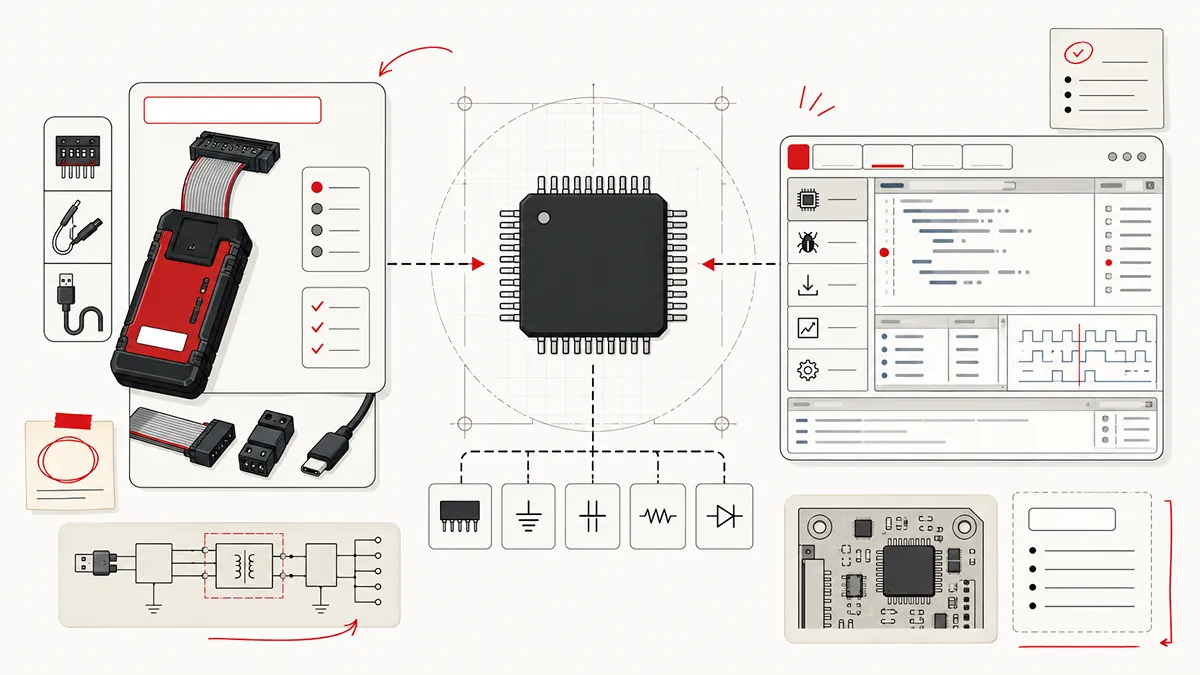
Introduction to Programming STM32F103C8T6
The STM32F103C8T6 is a widely adopted mid-density microcontroller built on the ARM Cortex-M3 RISC architecture. Operating at a 72 MHz clock frequency, it offers a robust balance of processing power and peripheral availability for industrial and embedded applications. Understanding how to properly interface with and program this device is a foundational skill for hardware engineers and embedded system developers.
Programming this microcontroller from scratch requires establishing a reliable communication link between your development environment and the chip's internal memory. While there are multiple ways to upload firmware, the industry-standard approach utilizes the Serial Wire Debug (SWD) protocol. This method bypasses the need for pre-installed bootloaders, granting direct access to the flash memory and enabling real-time hardware debugging. This guide outlines the professional workflow for programming the STM32F103C8T6 using an ST-Link V2 programmer and the official STM32CubeIDE environment.
What You Need Before You Start
Before initiating the programming sequence, ensure your workstation is equipped with the correct hardware and software tools. Using standardized, high-quality components minimizes initial connection variables and prevents potential electrical damage to the microcontroller.
Hardware requirements include:
- An STM32F103C8T6 development board or a custom PCB containing the microcontroller.
- An ST-Link V2 in-circuit debugger and programmer.
- Four female-to-female DuPont jumper wires for data and power connections.
- A standard USB cable to connect the ST-Link to your workstation.
Software requirements include:
- STM32CubeIDE: The official integrated development environment provided by STMicroelectronics.
- STM32CubeProgrammer: A standalone memory programming tool useful for verifying connections and erasing locked flash memory.
- The appropriate USB drivers for the ST-Link V2, which are typically bundled with the STM32CubeIDE installation.
ST-Link V2 Pinout and Wiring Setup
The ST-Link V2 communicates with the STM32F103C8T6 using the SWD interface, which requires only two data lines alongside power and ground. This protocol is specifically designed for ARM Cortex microcontrollers, providing a highly efficient debugging and programming channel. The STM32F103C8T6 operates on 3.3V logic, so it is critical to connect it to the 3.3V output of the ST-Link, not the 5V output.
Incorrect wiring is the leading cause of communication failures during the initial setup phase. Ensure the jumper wires are securely seated on both the programmer and the target board header pins.
| ST-Link V2 Pin | STM32F103C8T6 Target Pin | Function Description |
|---|---|---|
| 3.3V | 3.3V | Supplies power to the microcontroller during programming. |
| GND | GND | Establishes a common electrical ground. |
| SWDIO | SWDIO (PA13) | Handles bidirectional data transfer for the SWD protocol. |
| SWCLK | SWCLK (PA14) | Provides the clock signal for SWD data synchronization. |
BOOT0 and BOOT1 Settings Explained
The STM32F103C8T6 features a flexible startup architecture controlled by the hardware states of the BOOT0 and BOOT1 pins during the power-on reset phase. These pins determine the specific memory space from which the ARM Cortex-M3 processor fetches its initial instructions. Configuring these incorrectly will prevent the microcontroller from executing your uploaded firmware.
The BOOT0 pin is the primary configuration selector, while BOOT1 serves as a secondary modifier. For standard development boards, these are typically controlled via physical jumper caps.
| BOOT0 State | BOOT1 State | Boot Mode | Use Case |
|---|---|---|---|
| 0 (Low) | x (Don't Care) | Main Flash Memory | Standard operation; runs the user program uploaded via ST-Link . |
| 1 (High) | 0 (Low) | System Memory | Activates the factory bootloader for programming via USART . |
| 1 (High) | 1 (High) | Embedded SRAM | Used for specialized debugging and running code directly from RAM . |
When programming via the ST-Link V2 using SWD, the boot mode does not restrict the programmer's ability to write to the flash memory. However, to ensure the microcontroller immediately runs your new code after a reset, you must set the BOOT0 jumper to 0 (Low).
Setting Up STM32CubeIDE and STM32CubeProgrammer
STM32CubeIDE integrates hardware configuration and code generation into a single unified workspace. Establishing a project correctly ensures that the compiler targets the specific register map of the STM32F103C8T6.
Follow these configuration steps to initialize your software environment:
- Open STM32CubeIDE and navigate to File → New → STM32 Project.
- In the MCU/MPU Selector window, type "STM32F103C8" into the part number search bar and select the exact package match.
- Once the Device Configuration Tool (the graphical pinout view) loads, locate the "System Core" dropdown on the left pane and select "SYS".
- Under the "Debug" dropdown menu, you must select "Serial Wire". This action assigns the PA13 and PA14 pins to the SWD interface. Failing to enable this will cause the MCU to disable its programming pins immediately upon executing your code, locking you out of subsequent programming attempts.
- Navigate to the "RCC" section and configure your High-Speed Clock (HSE) if you intend to use an external crystal oscillator.
Save the configuration file. The IDE will automatically generate the foundational C code required to initialize the ARM processor and the selected peripherals.
How to Flash Your First Program to STM32F103C8T6
With the hardware wired and the software environment configured, you are ready to compile and upload firmware to the microcontroller. In STM32CubeIDE, the compilation and flashing processes are tightly integrated into the debugging workflow.
Steps to flash the microcontroller:
- Click the "Build" icon (the hammer symbol) in the top toolbar to compile your C code into an executable binary. Check the console output to ensure there are no syntax errors.
- Click the "Run" icon (the green play button) or the "Debug" icon (the bug symbol) to initiate the flashing sequence.
- The IDE will prompt you to configure the Run/Debug settings. Ensure the debugger tab is set to use the ST-LINK probe with the SWD interface.
- Click "OK" to commence the upload. The ST-Link V2 will erase the necessary flash memory sectors and write your compiled binary directly to the chip.
Upon successful execution, the IDE console will display "Download verified successfully". Press the physical reset button on your board to begin running the new firmware.
Troubleshooting ST-Link Connection Errors
Interfacing with embedded hardware frequently involves connection hurdles. When the ST-Link fails to communicate with the STM32F103C8T6, the IDE typically throws a generic "No device found" or "Target not found" error. This requires a systematic diagnostic approach to identify the root cause.
Common issues and their resolutions:
- Disabled SWD Pins: If a previously flashed program did not have "Serial Wire" enabled in the SYS settings, the MCU turns off the SWDIO and SWCLK pins on startup. To recover the chip, hold down the physical Reset button on the board, click "Run" in CubeIDE, and release the Reset button exactly when the IDE console indicates it is connecting to the target.
- UNEXPECTED idcode: This error, such as expected 1 of 1: 0x1ba01477, often occurs when the physical chip is a third-party clone (like a CS32 or CH32) rather than an original STMicroelectronics product. You may need to manually adjust the OpenOCD configuration files in the IDE to accept the alternate ID code.
- Insufficient Power: If the microcontroller is drawing power from an external circuit and the ST-Link simultaneously, ground loops or voltage drops can interrupt the SWD clock signal. Ensure a single, stable 3.3V power domain is used during programming.
- Outdated ST-Link Firmware: The programmer itself runs internal firmware. Use the STM32CubeProgrammer tool to connect to the ST-Link and perform a firmware update before attempting to flash the target board again.
ST-Link vs USB Bootloader
Engineers often evaluate whether to program the STM32F103C8T6 directly via its built-in micro-USB port or through the external ST-Link V2. Both methods achieve the goal of placing executable code into the flash memory, but they serve entirely different development stages and architectural requirements.
The SWD method using the ST-Link V2 is a bare-metal approach. It requires dedicated hardware but grants absolute control over the microcontroller, including the ability to set breakpoints, inspect register values, and halt code execution in real-time.
Conversely, the USB Bootloader method requires flashing a secondary bootloader program (such as the Maple bootloader) into the MCU's flash memory first. Once installed, developers can upload application code directly through a standard USB cable. While this eliminates the need for an external programmer for future updates, it consumes a portion of the available flash memory and entirely removes the capability for real-time hardware debugging. For professional industrial applications, the ST-Link V2 SWD method remains the mandatory standard.
Submit Your STM32 BOM for Sourcing Support
Developing robust embedded systems requires not only technical programming expertise but also a reliable supply chain. As hardware designs mature from prototype testing with the ST-Link V2 into mass production, sourcing genuine, traceable components becomes critical to project success. Supply chain volatility, unauthorized clones, and component obsolescence can severely impact industrial manufacturing timelines.
Vigor Components operates as a professional independent electronic components distributor, bridging the gap between engineering needs and global procurement realities. We provide authentic sourcing solutions for the STM32F103C8T6 and related microcontrollers, backed by rigorous quality inspection processes and clear traceability documentation.
If you are preparing for production or facing shortages with your current suppliers, submit your comprehensive Bill of Materials (BOM) to our procurement team. Our experts will review your MPNs, target quantities, and delivery requirements to provide a secure, verified quotation and proactive lifecycle management support.
Frequently Asked Questions
Can I program the STM32F103C8T6 using the Arduino IDE?
Yes, the STM32F103C8T6 can be programmed using the Arduino IDE, but it requires a completely different software workflow. You must install a dedicated STM32 board support package (often referred to as STM32duino) via the Arduino Board Manager. While accessible for rapid prototyping, it adds abstraction layers that make low-level peripheral configuration and real-time debugging more difficult compared to the native STM32CubeIDE environment.
What is the default clock speed after a fresh flash?
If you do not explicitly configure the clock tree in the STM32CubeIDE Device Configuration Tool, the STM32F103C8T6 defaults to using its internal 8 MHz RC oscillator (HSI). You must actively enable the PLL (Phase-Locked Loop) settings in the software to reach the maximum 72 MHz operating frequency.
Why does my program disappear after I cycle the power?
If your code runs successfully when initiated by the ST-Link but fails to boot when the system is powered off and on again, your BOOT0 pin is likely configured incorrectly. Ensure the BOOT0 jumper is tied to GND (0) so the microcontroller knows to execute code from the main flash memory upon startup.