
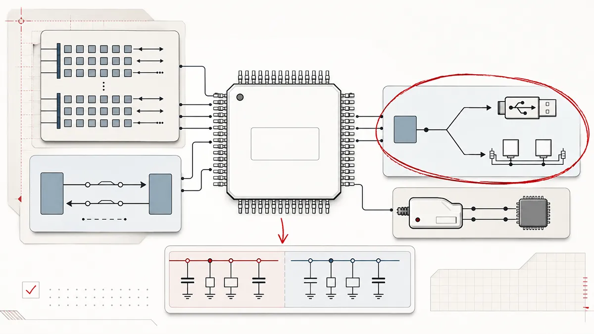
For embedded systems engineers and procurement specialists, the STM32F103C8T6 remains a cornerstone of the 32-bit microcontroller market in 2026. Manufactured by STMicroelectronics, this medium-density performance line MCU strikes a highly sought-after balance between computational power, peripheral integration, and cost-efficiency.
However, designing reliable printed circuit boards (PCBs) and sourcing authentic silicon requires moving beyond surface-level specs and diving into the official datasheet's internal architecture. This guide provides an authoritative breakdown of the STM32F103C8T6 pinout, critical electrical characteristics, and strategies to secure genuine inventory.
What is the STM32F103C8T6 MCU?
A Microcontroller Unit (MCU) is essentially a compact integrated circuit designed to govern a specific operation in an embedded system, functioning as a complete computer on a single chip. The STM32F103C8T6 is built on the 32-bit ARM® Cortex®-M3 RISC core operating at a maximum frequency of 72 MHz. Delivering 1.25 DMIPS/MHz at zero wait states, it is designed specifically for demanding, deterministic real-time applications.
The "C8" designation indicates that the silicon embeds 64 KB of Flash memory and 20 KB of SRAM. While hobbyists recognize it from "Blue Pill" development boards, its true B2B value lies in its complex internal bus matrix. The architecture connects a high-speed AHB bus to two APB buses, ensuring that heavy DMA (Direct Memory Access) transfers do not stall the CPU during critical sensor data acquisition.
STM32F103C8T6 Pinout Configuration
Packaged in a 48-pin LQFP (Low-Profile Quad Flat Package) with a tight 0.5 mm pitch, the MCU provides up to 37 individually mapable General Purpose I/O (GPIO) pins.
Unlike simpler 8-bit microcontrollers, the STM32F103C8T6 utilizes heavy pin multiplexing. For example, pins PA9 and PA10 function natively as standard GPIOs, but they must be mapped to Alternate Functions (AF) to operate as USART1_TX and USART1_RX. Furthermore, PA11 and PA12 handle the USB 2.0 interface (D- and D+), but they share multiplexing channels with the CAN bus; hardware engineers must design the PCB knowing that USB and CAN cannot be utilized simultaneously on these specific pins without complex external switching logic.
Understanding Power Pins and 5V Tolerant Architecture
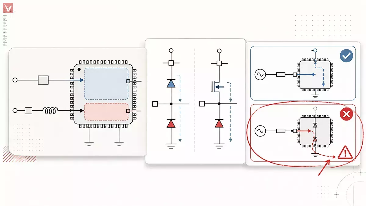
To correctly interpret the STM32 datasheet, engineers must understand the distinct power domains:
/
: The primary digital power supply.
(Voltage at the Drain) provides the positive 3.3V logic power, while
/
: The isolated analog power supply. To prevent digital switching noise from corrupting ADC readings,
A major engineering advantage of the STM32F103C8T6 is its 5V tolerant pins, identified by the "FT" label in the datasheet. These pins allow direct interfacing with legacy 5V logic sensors without utilizing external level-shifting ICs.
However, engineers must understand the internal architecture of these pins:
- Internal Clamping Diodes: Standard GPIOs have two protection diodes (one clamping to
- Power Dependency: A pin is only 5V tolerant when the MCU is actively powered. Applying 5V to an FT pin when
violates the absolute maximum voltage rating, causing parasitic current injection and permanent silicon damage.
- Injection Current Limits: The absolute maximum injected current
across all I/O pins must never exceed
.
Key Specifications from the Datasheet
To ensure hardware longevity, designers must respect the boundaries of the absolute maximum ratings. Below are the verified electrical characteristics directly from the STMicroelectronics database.
| Parameter | Datasheet Specification | Engineering Note |
|---|---|---|
| Operating Voltage |
2.0 V to 3.6 V | Core logic power supply; 3.3V is standard. |
Max Current per GPIO  |
25 mA (Absolute Maximum) | Recommended continuous load is  per pin. per pin. |
Total Chip Current  |
150 mA (Absolute Maximum) | Total combined source/sink current cannot exceed this limit. |
| Standby Power Consumption |  (Typical at 3.3V) (Typical at 3.3V) |
Requires proper configuration of the PWR control register. |
| Operating Temperature | -40°C to +85°C | Industrial grade rating for standard F103 variants. |
Common Applications of STM32F103C8T6
In the B2B sector, this microcontroller is heavily integrated into precise power conversion and motion control hardware.
One of its most powerful features is TIM1, an advanced-control 16-bit timer specifically engineered for three-phase motor control. By configuring the BDTR (Break and Dead-Time Register), engineers can generate complementary PWM signals with hardware-enforced dead-time. For example, setting the DTG (Dead-Time Generator) register allows the MCU to automatically insert microsecond delays between the switching of high-side and low-side MOSFETs in an H-bridge topology. This prevents catastrophic shoot-through currents in solar inverters, UPS systems, and BLDC motor drivers without requiring any CPU overhead.
How to Avoid Counterfeit MCU Chips
The global popularity of the STM32 series has led to a severe influx of counterfeit clones (such as CKS32 or APM32) disguised with laser-etched ST logos. Installing fake silicon compromises device safety and voids hardware warranties. Use these EEAT-backed technical methods to verify authenticity:
- Query the DBGMCU_IDCODE: Using an ST-Link debugger, read the MCU's internal debug registry. A genuine medium-density STM32F103 chip will return the exact value 0x410.
- Inspect the SW-DP ID: Authentic ST chips commonly report an SWD identification code of 0x1BA01477 or 0x2BA01477. Clones frequently present mismatched identifiers.
- Test the Flash Memory Limits: While the C8T6 is officially binned for 64 KB, genuine ST silicon often physically contains 128 KB. Clones frequently fail memory write-tests beyond the 64 KB boundary.
Ready to Source STM32F103C8T6 MCUs?
Supply chain integrity is just as critical as electrical engineering. Sourcing from unverified third-party marketplaces drastically increases the risk of receiving counterfeit or factory-rejected batches.
At Vigor Components, we specialize in distributing authentic, fully traceable electronic components. Whether you require samples for prototyping or Tape and Reel (TR) packaging for high-volume automated SMT assembly, our strict inventory QA ensures you only receive legitimate STMicroelectronics silicon.
Frequently Asked Questions
Can I program the STM32F103C8T6 with Arduino IDE?
Yes. By installing the STM32duino core, developers can write C++ code in the Arduino IDE and flash it via an ST-Link V2 programmer or a USB-to-Serial converter.
What is the difference between STM32F103C8T6 and STM32F103C8T6TR?
The hardware is physically and electrically identical. The "TR" suffix simply denotes "Tape and Reel" packaging, which is the standard format required for automated pick-and-place manufacturing machines.
Does the STM32F103C8T6 have a built-in DAC?
No. While it features two advanced 12-bit ADCs (Analog-to-Digital Converters), the medium-density F103 line lacks a built-in DAC. You must implement an external DAC IC or utilize a filtered PWM signal for analog output.
Is an external crystal oscillator strictly required?
No. The MCU contains an internal 8 MHz RC oscillator (HSI) sufficient for basic logic. However, if your application utilizes the CAN bus or USB 2.0 interfaces, an external 8 MHz crystal (HSE) is strictly required to meet the precise timing tolerances of those communication protocols.
What is the max current output per GPIO pin?
The absolute maximum rating is 25 mA per pin. However, for safe, long-term continuous operation, the datasheet recommends not exceeding ±8mA\pm 8\mathrm{mA}±8mA per GPIO, while ensuring total chip current does not surpass 150 mA.
Can the STM32F103C8T6 run FreeRTOS?
Yes. With 20 KB of SRAM, the chip comfortably supports the FreeRTOS real-time kernel. The scheduler and task stacks leave ample memory for standard peripheral handling and application logic.