
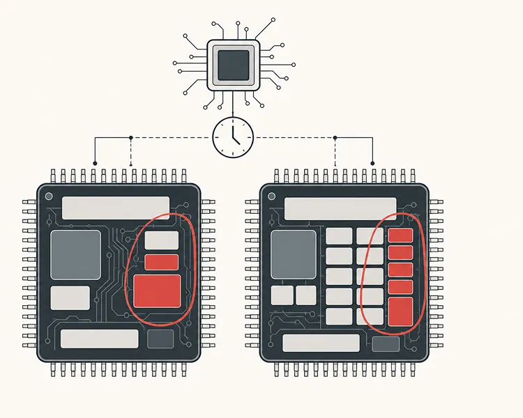
STM32F103C6T6 and STM32F103C8T6 use the same 48-pin LQFP package, Arm Cortex-M3 architecture, and 72 MHz maximum CPU frequency. The real design decision is not CPU speed: it is whether the C6T6’s 32 KB Flash and 6 KB SRAM are enough, or whether the C8T6’s 64 KB Flash and 20 KB SRAM provide necessary firmware and peripheral headroom.
For a production BOM, treat a C6T6 substitution as an engineering validation task rather than a purchasing-only decision. ST identifies STM32F103x6 as a low-density device and STM32F103x8 as a medium-density device; their resource differences extend beyond memory in the complete family specification.
STM32F103C6T6 vs STM32F103C8T6 Overview
The STM32F103C6T6 is the 48-pin LQFP version of ST’s low-density STM32F103x6 family. The STM32F103C8T6 is the corresponding 48-pin LQFP version in the medium-density STM32F103x8 family.
In ST’s ordering scheme:
- STM32F103 identifies the STM32F1 performance-line MCU family.
- C identifies the 48-pin device option.
- 6 represents 32 KB of Flash; 8 represents 64 KB of Flash.
- T specifies the LQFP package.
- 6 specifies the industrial temperature range of -40 °C to +85 °C.
| Parameter | STM32F103C6T6 | STM32F103C8T6 |
|---|---|---|
| Device density | Low density | Medium density |
| CPU core | Arm Cortex-M3 | Arm Cortex-M3 |
| Maximum CPU frequency | 72 MHz | 72 MHz |
| Flash memory | 32 KB | 64 KB |
| SRAM | 6 KB | 20 KB |
| Package | LQFP48, 7 × 7 mm | LQFP48, 7 × 7 mm |
| Operating supply | 2.0 V to 3.6 V | 2.0 V to 3.6 V |
| Temperature suffix “6” | -40 °C to +85 °C | -40 °C to +85 °C |
Memory Differences: 32 KB vs 64 KB Flash
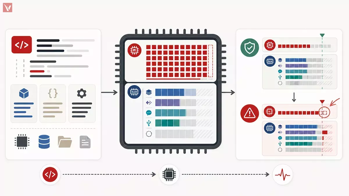
Flash stores the application firmware, constant tables, bootloader, and embedded libraries. SRAM holds runtime variables, call stacks, peripheral buffers, DMA buffers, and—in RTOS-based designs—individual task stacks.
The C8T6 doubles Flash capacity and provides 20 KB SRAM, compared with 6 KB SRAM on the C6T6. This SRAM difference is often more important than the Flash difference. A project may compile within 32 KB Flash but still become unstable on the C6T6 if stack usage, USB buffers, serial receive buffers, or DMA allocations exceed available SRAM.
Before considering C8T6-to-C6T6 migration, verify:
- Flash usage after linking, including bootloader and reserved Flash areas.
- Static .data and .bss consumption.
- Worst-case stack depth, especially within interrupt service routines.
- Heap usage, if dynamic allocation is enabled.
- USB, CAN, UART, ADC, or DMA buffer allocations.
- Required margin for future firmware maintenance.
Do not use 100% of the stated memory capacity as a production target. The available margin should cover compiler changes, diagnostic features, protocol updates, and unexpected stack growth.
Peripheral and Interface Comparison
At the 48-pin C-package level, both parts support two 12-bit ADCs, USB full-speed, CAN 2.0B Active, one SPI, one I2C, two USARTs, one advanced-control timer, and two general-purpose timers.
However, ST’s medium-density family has a broader peripheral ceiling across its package options: up to seven timers, two SPI interfaces, two I2C interfaces, and three USARTs. The low-density family is specified with fewer timers and communication interfaces. Therefore, engineers should compare the exact STM32F103C6T6 and STM32F103C8T6 pinout and peripheral table—not only family-level marketing summaries.
| Design Area | STM32F103C6T6 | STM32F103C8T6 | Engineering Impact |
|---|---|---|---|
| Debug | SWD and JTAG | SWD and JTAG | The same ST-Link workflow can be used. |
| ADC | 2 × 12-bit ADCs | 2 × 12-bit ADCs | Validate channel availability on the LQFP48 pinout. |
| USB | USB 2.0 full-speed device | USB 2.0 full-speed device | USB firmware memory demand may favor the C8T6. |
| CAN | CAN 2.0B Active | CAN 2.0B Active | External CAN transceiver is still required. |
| GPIO | 37 I/Os in C-package family table | 37 I/Os in C-package family table | Package-level pin compatibility must still be checked. |
Cost Analysis for Bulk Manufacturing
The C6T6 may offer a lower purchase cost than the C8T6, but a lower unit price does not automatically create a lower total BOM cost. Pricing changes with order quantity, authorized versus independent distribution, package condition, lead time, and regional availability.
A responsible cost-down review compares the component savings against validation cost and production risk:
- Confirm that the exact LQFP48 footprint and pin assignment are unchanged.
- Rebuild the released firmware using the C6T6 linker memory limits.
- Run functional, stress, startup, communication, and production-programming tests.
- Check whether the firmware can retain a safe Flash and SRAM margin.
- Obtain quotes based on the required quantity, date code, packaging, and delivery schedule.
For long-running production programs, a memory downgrade that eliminates future firmware flexibility can cost more than the initial MCU saving.
Firmware Compatibility and Migration
ST states that STM32F103 low-, medium-, and high-density devices are pin-to-pin, software, and feature compatible within the family framework. It also describes lowand high-density devices as extensions of the medium-density family.
That statement supports a practical migration path, but it does not mean every C8T6 firmware image will run unchanged on a C6T6. The C6T6 has half the Flash and less SRAM. Firmware built for the C8T6 may fail at link time, crash from stack overflow, or lose functionality when code and buffer sizes are reduced.
A controlled migration should include:
- Select the correct C6T6 startup file and linker script.
- Compile with warnings enabled and review the linker memory report.
- Test boot mode, SWD programming, reset behavior, and watchdog recovery.
- Validate all active interfaces under realistic bus traffic.
- Measure memory use under peak runtime conditions, not only at startup.
Can STM32F103C6T6 Replace STM32F103C8T6 Directly?
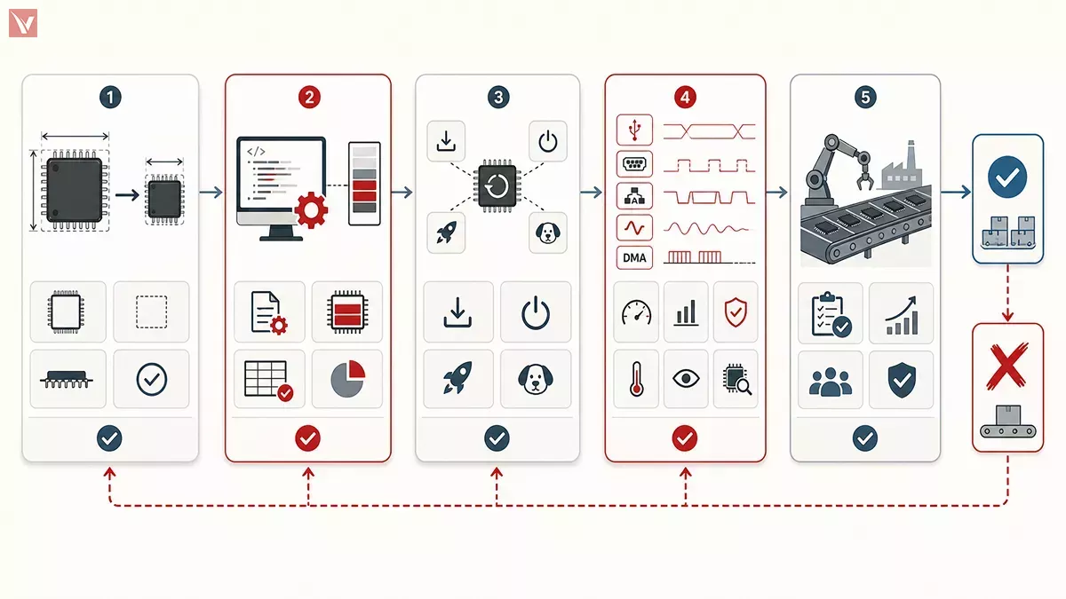
Physically, it can be a compatible option when both designs use the matching LQFP48 package. Functionally, it is only suitable when the firmware and runtime memory requirements fit the C6T6 limits.
The C6T6 is a reasonable replacement when the existing design has compact firmware, limited buffers, no memory-intensive middleware, and verified resource margin. It is a poor cost-down candidate when the C8T6 design uses USB stacks, extensive serial protocols, logging, large lookup tables, bootloaders, RTOS tasks, or planned feature expansion.
Looking for Reliable MCU Supply Chains?
A valid MCU quote should identify more than a unit price. For STM32F103C6T6 or STM32F103C8T6 purchasing, request:
- Full manufacturer part number and package.
- Condition and packaging format, such as factory reel, tray, cut tape, or surplus stock.
- Available quantity and date-code information.
- Lead time, quotation validity, and delivery destination.
- Traceability documentation or inspection information where available.
- A clear statement that any alternative MCU requires customer-side electrical, firmware, and qualification approval.
An experienced BOM review can identify whether the C6T6 memory limits make a cost-down technically realistic before procurement changes the approved manufacturer list.
Frequently Asked Questions
What does the “T6” suffix mean?
In STM32F103C8T6, T identifies the LQFP package and the final 6 identifies ST’s -40 °C to +85 °C industrial temperature range. The C indicates the 48-pin option, while 6 or 8 before the package letter identifies Flash density.
Are power-consumption differences significant?
ST publishes power-consumption data by device family and operating conditions, not as a simple C6T6-versus-C8T6 headline figure. Current depends on clock frequency, voltage, temperature, enabled peripherals, I/O loading, program execution, and memory access configuration.
Can the same ST-Link program both devices?
Yes. Both devices include serial wire debug and JTAG interfaces, so the same ST-Link hardware and standard STM32 programming workflow can be used.
What happens when C8T6 firmware exceeds C6T6 memory?
A correctly configured C6T6 linker script should report a Flash or SRAM overflow during the build. If memory limits are configured incorrectly, the firmware may program but behave unpredictably, especially when runtime stack or buffer demand exceeds SRAM.
Are GD32 devices direct equivalents?
GD32 alternatives should not be treated as automatic replacements. Engineers must verify package, pinout, operating conditions, boot behavior, peripheral registers, electrical limits, firmware toolchain behavior, and final product qualification before approving a cross-brand substitution.