
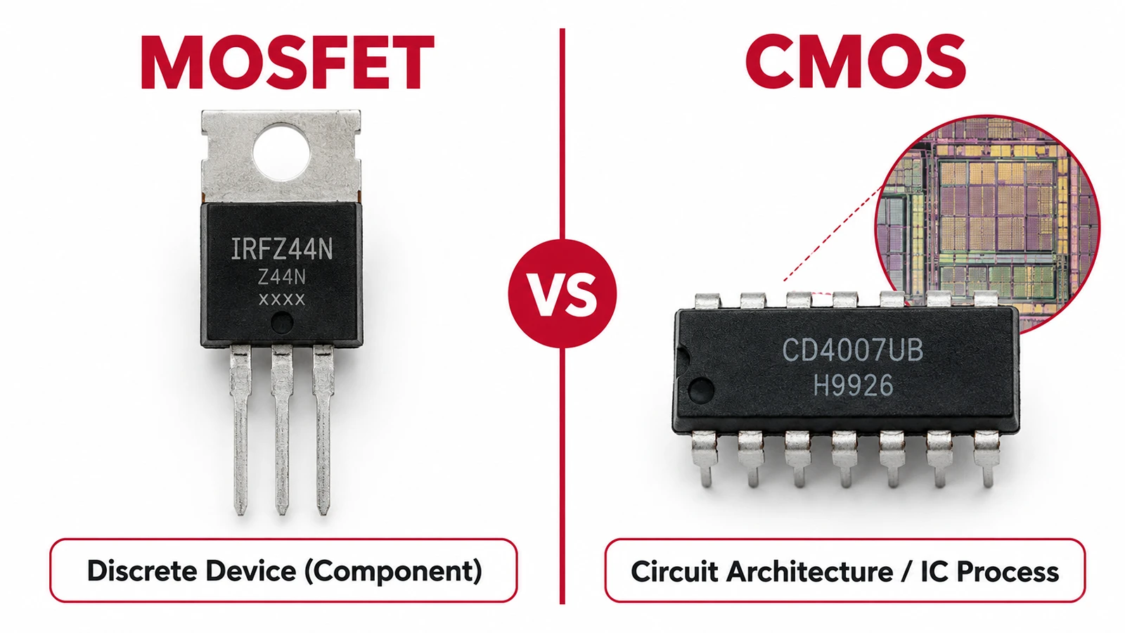
No, MOSFETs and CMOS are not the same thing, even though they are closely related in semiconductor electronics. A MOSFET (Metal-Oxide-Semiconductor Field-Effect Transistor) is an individual transistor device that acts as a voltage-controlled electronic switch or amplifier. In contrast, CMOS (Complementary Metal-Oxide-Semiconductor) is a circuit design architecture and fabrication process that combines symmetrical pairs of N-channel (NMOS) and P-channel (PMOS) MOSFETs on a single silicon substrate. Understanding the difference between CMOS vs. MOSFET helps engineers and component buyers distinguish between discrete power switches and low-power digital logic integrated circuits (ICs) during schematic design and Bill of Materials (BOM) sourcing.
Are MOSFETs and CMOS the Same Thing?
When asking "are MOSFETs and CMOS same," the fundamental distinction comes down to component hierarchy: one is an individual building block, while the other is a circuit topology built from those blocks.
Every CMOS circuit is constructed using MOSFETs, meaning CMOS technology cannot exist without MOSFETs. However, a single MOSFET by itself is never a CMOS circuit. A MOSFET can function independently as a standalone 3-pin discrete power transistor on a printed circuit board (PCB), or millions of microscopic MOSFETs can be wired together in complementary pairs inside an integrated circuit to form a CMOS device.
| Hierarchy Level | Terminology | Engineering Definition | Typical Physical Form |
|---|---|---|---|
| 1. Individual Device Level | MOSFET (NMOS or PMOS) | A single voltage-controlled field-effect transistor with Gate, Source, and Drain terminals. | Standalone discrete packages (e.g., TO-220, SO-8, SOT-23) or a single microscopic transistor cell on a silicon die. |
| 2. Basic Circuit Cell Level | Complementary MOS Pair | One P-channel MOSFET and one N-channel MOSFET connected in a push-pull configuration (the basic CMOS inverter). | Matched transistor arrays (such as the Texas Instruments CD4007UB) or internal logic gates. |
| 3. System / IC Process Level | CMOS Technology | Complete digital or mixed-signal integrated circuits fabricated using complementary NMOS and PMOS networks. | Logic ICs (74HC series), microcontrollers (MCUs), SRAM, and CMOS image sensors. |
What Is a MOSFET? Structure, Types, and Standalone Role
A MOSFET (Metal-Oxide-Semiconductor Field-Effect Transistor) is a four-terminal semiconductor device consisting of a Gate (G), Source (S), Drain (D), and Body/Substrate (B) (in discrete three-pin packages, the body is typically internally shorted to the source). Unlike Bipolar Junction Transistors (BJTs), which require continuous base current to stay conductive, a MOSFET uses an insulated metal-oxide gate layer (typically silicon dioxide, \(V_{GS}\)). Applying a voltage across the Gate and Source ( \(V_{GS}\)) creates an electric field that modulates the conductivity of the semiconductor channel between the Drain and Source.
According to Texas Instruments Application Note AN-558 (Introduction to Power MOSFETs and Their Applications, SNVA008), MOSFETs operate in one of two modes:
- Enhancement-Mode MOSFETs (Normally Off): No conductive channel exists at \(V_{GS} = 0\text{ V}\) . The transistor blocks current until a sufficient gate voltage is applied. Virtually all modern digital logic MOSFETs and discrete power switches are enhancement-mode devices so that circuits remain safely off when unpowered.
- Depletion-Mode MOSFETs (Normally On): A conductive channel is physically implanted during manufacturing, allowing current to flow at \(V_{GS} = 0\text{ V}\) until a reverse gate bias pinches the channel closed.
N-Channel (NMOS) vs. P-Channel (PMOS) Operation
Within enhancement-mode MOSFETs, devices are categorized by the polarity of their charge carriers. When reviewing transistor and MOSFET schematic symbols, the direction of the substrate arrow indicates the channel type:
- N-Channel MOSFET (NMOS): Uses electrons as majority carriers. An enhancement-mode NMOS turns ON when the gate voltage is positive relative to the source and exceeds the gate threshold voltage ( \(V_{GS} > V_{GS(th)}\) ). Because electrons have higher mobility in silicon than holes, NMOS transistors achieve lower on-state resistance ( \(R_{DS(on)}\) ) and smaller die area for a given current rating. They are standard for low-side power switching and pull-down networks connected to ground (GND).
- P-Channel MOSFET (PMOS): Uses holes as majority carriers. An enhancement-mode PMOS turns ON when the gate voltage is negative relative to the source ( \(V_{GS} < V_{GS(th)}\) , where \(V_{GS(th)} \) is a negative value). PMOS devices are commonly used for high-side load switching and pull-up networks connected to the positive supply rail ( \(V_{DD}\) or \(V_{DD}\) ).
Discrete Power MOSFETs (Vertical Trench/DMOS) vs. Integrated Micro-MOSFETs (Lateral)
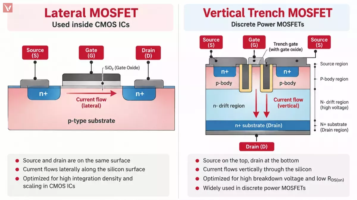
A critical distinction missing from most people is that a discrete power MOSFET on a power supply board is physically structured very differently from the microscopic MOSFETs inside a CMOS logic chip.
As documented in Texas Instruments AN-558 and Infineon's Designing with Power MOSFETs application notes:
- Lateral Planar MOSFETs (Used Inside CMOS ICs): The Source, Gate, and Drain terminals all sit horizontally on the top surface of the silicon wafer. Current flows parallel to the wafer surface. This horizontal layout makes it easy to interconnect millions of NMOS and PMOS transistors on a single die, but it results in higher channel resistance and limited voltage blocking capability.
- Vertical Power MOSFETs (Planar DMOS and Trench MOSFETs): Discrete power MOSFETs place the Source and Gate on the top surface and the Drain on the back side of the silicon die. Current flows vertically through the silicon drift region. This vertical architecture allows a discrete MOSFET to block tens to hundreds of volts ( \(BV_{DSS}\) ) while maintaining milliohm-level on-resistance ( \(R_{DS(on)}\) ) for high-current applications like DC-DC converter circuits.
What Is CMOS? How Complementary MOSFET Pairs Work Together
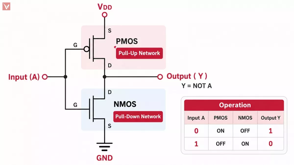
CMOS stands for Complementary Metal-Oxide-Semiconductor. As defined in Toshiba's official semiconductor technical documentation (What is a CMOS Logic IC?), a CMOS circuit combines p-channel MOSFETs and n-channel MOSFETs in complementary pairs to execute digital logic functions.
Instead of using resistive pull-up loads (which waste continuous heat whenever a switch is closed), CMOS places a PMOS transistor network between the positive power rail ( \(V_{DD}\)) and the output, and a complementary NMOS transistor network between the output and ground (GND).
Inside a Basic CMOS Inverter (Pull-Up PMOS + Pull-Down NMOS)
The simplest building block of all CMOS digital electronics is the CMOS Inverter (NOT Gate), which consists of exactly one PMOS transistor and one NMOS transistor:
              VDD (Positive Supply, Logic 1)
               |
             +---+ Source (S)
             |   |
    +-------o|   | PMOS (Pull-Up Network: ON when Input = Low)
    |  Gate  |   |
    |        +---+ Drain (D)
    |          |
Input (A) -----+---------- Output (Y = NOT A)
    |          |
    |        +---+ Drain (D)
    |  Gate  |   |
    +--------|   | NMOS (Pull-Down Network: ON when Input = High)
             |   |
             +---+ Source (S)
               |
              GND (Ground, Logic 0)
(Schematic representation based on standard CMOS inverter topology from Toshiba Logic Basics Chapter 2-1 and Texas Instruments CD4007UB Datasheet SCHS018C)
Here is how the complementary pair operates across logic states:
- When Input (A) is LOW ( \(0\text{ V} \) , Logic 0):
- NMOS State: The gate-to-source voltage of the bottom NMOS is \(V_{GS} = 0\text{ V}\) , which is below its positive threshold voltage. The NMOS remains OFF (open circuit to GND).
- PMOS State: Because the PMOS source is tied to \(V_{DD}\) , a \(0\text{ V}\) gate input results in a negative gate-to-source voltage ( \(V_{GS} = -V_{DD}\) ), strongly turning the PMOS ON.
- Result: The PMOS pulls the Output (Y) cleanly up to \(V_{DD}\) (Logic 1), while the turned-off NMOS blocks any direct current path to ground.
- When Input (A) is HIGH ( \(V_{DD}\) , Logic 1):
- PMOS State: With the gate at \(V_{DD}\) and the source at \(V_{DD}\) , the PMOS sees \(V_{GS} = 0\text{ V}\) and turns OFF (open circuit from \(V_{DD} \) ).
- NMOS State: The bottom NMOS sees \(V_{GS} = +V_{DD}\) , turning it ON.
- Result: The NMOS pulls the Output (Y) down to GND (Logic 0), while the turned-off PMOS blocks current from the supply rail.
Why CMOS Dominates Low-Power Digital Integrated Circuits
The primary engineering advantage of CMOS is near-zero static power dissipation. Because the PMOS and NMOS transistors operate in opposite (complementary) states, there is never a continuous direct path between \(V_{DD}\) and GND during a steady logic 0 or logic 1 state. The only current flowing when a CMOS gate is idle is sub-threshold and junction leakage current—typically in the nanoampere ( \(\text{nA}\)) or microampere ( \(\mu\text{A}\)) range.
As verified in Toshiba's Countermeasures for Reducing Switching Noise in CMOS Logic ICs (Section 9-1), CMOS circuits consume noticeable power only during dynamic switching transitions (when charging and discharging capacitive loads \(C_L\) at frequency \(f\), governed by \(P_{\text{dynamic}} = C_L \cdot V_{DD}^2 \cdot f\), plus a brief shoot-through current as the input voltage passes through the mid-rail region). This ultra-low static power allows engineers to pack billions of MOSFETs onto a single microprocessor, FPGA, or memory chip without melting the silicon die.
CMOS vs. MOSFET: Side-by-Side Technical Comparison
When comparing CMOS vs. MOSFET (or MOSFET vs. CMOS), it helps to evaluate how a standalone MOSFET component differs from a CMOS integrated circuit across electrical, structural, and application parameters.
| Comparison Dimension | MOSFET (Discrete / Device Level) | CMOS (Circuit / Process Level) |
|---|---|---|
| Full Term | Metal-Oxide-Semiconductor Field-Effect Transistor | Complementary Metal-Oxide-Semiconductor |
| Fundamental Nature | An individual semiconductor transistor component. | A circuit architecture and wafer fabrication process built from complementary MOSFET pairs. |
| Transistor Polarity | Uses either an N-channel (NMOS) or a P-channel (PMOS) channel per switch (some packages house dual FETs). | Always combines both N-channel (NMOS) and P-channel (PMOS) transistors in symmetrical push-pull pairs. |
| Primary Engineering Role | High-efficiency power switching, load driving, motor control, DC-DC regulation, and RF/analog amplification. | Digital logic gates (Inverters, NAND, NOR), microcontrollers, CPUs, SRAM, and image sensors. |
| Static Power Consumption | Dissipates continuous conduction power whenever turned ON (P = ID2 × RDS(on)). | Near-zero static power in steady '0' or '1' states; power is consumed primarily during state transitions. |
| Physical Silicon Structure | Typically uses vertical silicon structures (Planar DMOS or Trench) to support high voltage and high current. | Uses lateral planar or 3D FinFET structures optimized for high transistor density on a shared silicon die. |
| Typical Voltage & Current Scale | Voltage ratings (BVDSS) from 12V to >1,200V; continuous drain currents (ID) from hundreds of milliamps to >100A. | Operating supply voltages (VDD/VCC) typically 1.2V to 18V; output pin drive currents typically 1mA to 24mA. |
| Representative Examples | Discrete N-channel/P-channel Power MOSFETs, Small-Signal FETs. | TI CD4000 series (e.g., CD4007UB), 74HCxx logic gates, CMOS SRAM, STM32 MCUs. |
Why Do People Often Confuse MOSFETs and CMOS?
If a MOSFET is a single transistor and CMOS is a multi-transistor circuit topology, why do engineers, students, and purchasing teams frequently encounter confusion between the two terms? Three practical factors explain the overlap:
- Shared "MOS" Terminology: Both acronyms share Metal-Oxide-Semiconductor, referring to the physical stack of a conductive gate, an insulating oxide layer, and a doped semiconductor channel. In casual conversation, people sometimes say "a CMOS transistor" when they actually mean "a MOSFET fabricated inside a CMOS process."
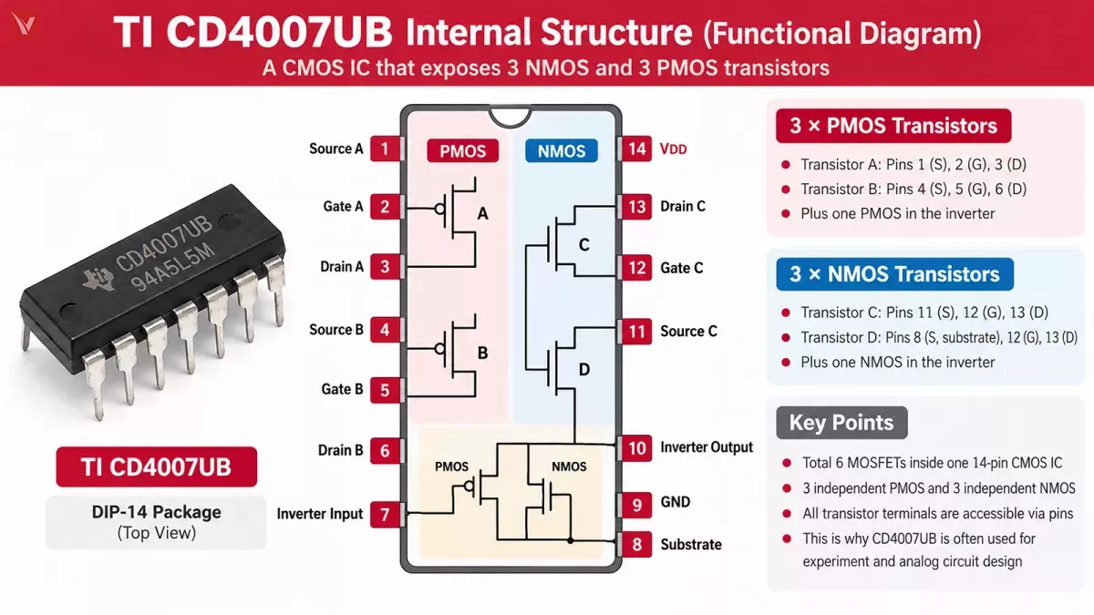
- "Bridge" Components That Expose Raw CMOS Pairs (e.g., TI CD4007UB): Certain classic integrated circuits blur the line between discrete MOSFETs and pre-wired CMOS logic gates. A prime verified example is the Texas Instruments CD4007UB (CMOS Dual Complementary Pair Plus Inverter, Datasheet SCHS018C). Packaged in a 14-pin PDIP, SOIC, or TSSOP housing, the CD4007UB consists of three N-channel and three P-channel enhancement-mode MOS transistors. Rather than locking all transistors into fixed logic gates internally, TI brings the individual Gate, Source, and Drain terminals of the complementary pairs out to external package pins. According to the TI CD4007UB datasheet, the device operates from \(3\text{ V}\) to \(18\text{ V}\) , exhibits a typical propagation delay of \(30\text{ ns}\) (at \(V_{DD} = 10\text{ V}\) ), and draws a maximum input leakage current of just \(100\text{ nA}\) at \(18\text{ V}\) and \(25^\circ\text{C}\) ( \(1\text{ }\mu\text{A}\) max across \(-55^\circ\text{C}\) to \(125^\circ\text{C}\) ).
- Colloquial Hardware Naming ("CMOS Battery" and "CMOS Sensor"): In personal computers, technicians routinely refer to the motherboard backup coin cell as the "CMOS battery." The battery itself is not a semiconductor; it is typically a CR2032 lithium coin cell battery that supplies standby microamps to a low-power CMOS SRAM chip storing BIOS settings and the real-time clock (RTC). Similarly, in digital cameras, a "CMOS sensor" refers to an active-pixel image sensor whose pixel readout amplifiers and analog-to-digital converters are manufactured on a CMOS IC process.
How CMOS ICs and Discrete MOSFETs Work Together in a Circuit
In real-world PCB design and BOM procurement, you do not choose between MOSFET vs. CMOS as mutually exclusive alternatives—instead, you use CMOS integrated circuits as the low-power control brain and discrete power MOSFETs as the high-current switching muscle.
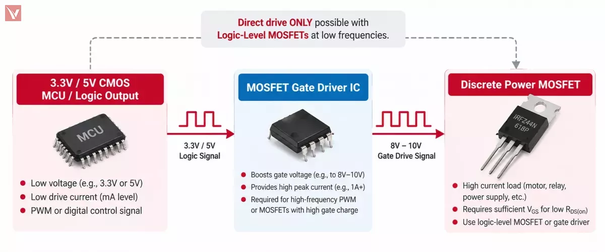
For example, in an industrial motor controller or buck and boost converters, a CMOS microcontroller or logic gate generates a pulse-width modulation (PWM) signal, which then switches a discrete N-channel power MOSFET to control the heavy load. However, connecting a CMOS logic output directly to a discrete power MOSFET gate introduces two critical engineering constraints that must be verified in manufacturer datasheets.
1. Voltage Matching: Standard Power MOSFETs vs. Logic-Level MOSFETs
A common design mistake is checking only the Gate Threshold Voltage ( \(V_{GS(th)}\)) on a power MOSFET datasheet—often listed around \(2\text{ V}\) to \(4\text{ V}\)—and assuming a \(3.3\text{ V}\) or \(5\text{ V}\) CMOS logic pin can fully turn it on.
- \(V_{GS(th)}\) only specifies the voltage where the MOSFET barely begins to conduct a tiny test current (typically \(250\text{ }\mu\text{A}\) ).
- Many standard high-voltage silicon power MOSFETs require a gate drive voltage of \(V_{GS} = 8\text{ V}\text{ to }10\text{ V}\) to reach their rated minimum on-resistance ( \(R_{DS(on)}\) ). Driving such a MOSFET directly from a \(3.3\text{ V}\) CMOS output leaves the transistor partially resistive, causing severe \(I_D^2 \times R_{DS(on)\) overheating.
- The Engineering Solution: If driving a discrete MOSFET directly from a \(3.3\text{ V}\) or \(5\text{ V}\) CMOS IC at low switching frequencies, you must specify a Logic-Level MOSFET—a device whose datasheet explicitly guarantees a low maximum \(R_{DS(on)}\) at \(V_{GS} = 4.5\text{ V}\) , \(3.3\text{ V}\) , or \(2.5\text{ V}\) .
2. Current Drive & Gate Charge (Qg): When You Need a Gate Driver IC
Even if the gate voltage matches, a power MOSFET behaves like a nonlinear capacitor at its gate terminal. According to Infineon's Power MOSFET Basics application note (Page 8), a MOSFET's switching speed is governed by how quickly the driving circuit can charge and discharge its internal parasitic capacitances:
- Input Capacitance: \(C_{iss} = C_{GS} + C_{GD}\) (with drain-source shorted)
- Reverse Transfer (Miller) Capacitance: \(C_{rss} = C_{GD}\)
- Output Capacitance: \(C_{oss} = C_{DS} + C_{GD}\)
Standard CMOS logic ICs have very limited output current drive—for instance, the Texas Instruments CD4007UB has a maximum output low/high current ( \(I_{OL}\)/ \(I_{OH}\)) of only \(\pm 4\text{ mA}\).
Infineon's application note provides a clear quantitative comparison for a discrete power MOSFET with a total gate charge of \(Q_g = 20\text{ nC}\):
- Driven by \(1\text{ mA}\) (weak logic output): The turn-on transition takes \(t = \frac{Q_g}{I_G} = \frac{20\text{ nC}}{1\text{ mA}} = 20\text{ }\mu\text{s}\) . During those \(20\text{ }\mu\text{s}\) , the MOSFET experiences simultaneous high voltage and high current, generating high switching losses in PWM circuits.
- Driven by \(1\text{ A}\) (dedicated Gate Driver IC): The turn-on transition drops to \(t = \frac{20\text{ nC}}{1\text{ A}} = 20\text{ ns}\) —one thousand times faster.
Furthermore, when designing with CMOS logic ICs on the control side, Toshiba's CMOS Logic Usage Considerations (Section 9-1) emphasizes a strict hardware rule: never leave unused CMOS input pins floating. Because MOSFET gates have extremely high input impedance, an unconnected CMOS input pin can float to an intermediate voltage from board noise, turning both the internal PMOS and NMOS partially ON simultaneously and causing excessive supply current and switching noise. Always tie unused CMOS logic inputs directly (or via a resistor) to \(V_{CC}/V_{DD}\) or GND.
Component Selection & BOM Categorization Matrix
Use the table below to classify components and verify critical datasheet parameters when building or sourcing a BOM:
| Engineering / BOM Requirement | Component Category to Select | Critical Datasheet Parameters to Verify | Verified Engineering Reason |
|---|---|---|---|
| High-current load switching, motor drive, or DC-DC power stage | Discrete Power MOSFET (N-channel or P-channel) | • Drain-Source breakdown voltage (BVDSS) • Continuous drain current (ID) • On-resistance (RDS(on)) at specified VGS • Total gate charge (Qg) • Thermal resistance (RθJC / RθJA) |
Ensures the vertical power MOSFET can block system voltage margins and carry load current without exceeding junction temperature limits (TJ). |
| Low-power digital state logic, signal inversion, or buffering | CMOS Logic IC (e.g., 74HC series, TI CD4000 series) | • Supply voltage range (VCC or VDD) • Quiescent supply current (ICC) • Propagation delay (tpd / tPHL / tPLH) • Input high/low voltage thresholds (VIH / VIL) • Output drive current (IOH / IOL) |
Confirms logic-level voltage compatibility across the signal chain and verifies ultra-low standby power consumption. |
| Direct low-frequency load switching from a 3.3V / 5V CMOS MCU pin | Logic-Level Discrete MOSFET | • RDS(on) explicitly rated at VGS = 2.5V, 3.3V, or 4.5V • Maximum VGS(th) well below MCU rail • Input capacitance (Ciss) |
Prevents partial turn-on and thermal runaway when driven directly by low-voltage CMOS logic rails without a level shifter. |
| High-frequency PWM switching of a power MOSFET from a CMOS controller | CMOS-Input MOSFET Gate Driver IC + Discrete Power MOSFET | • CMOS/TTL input logic threshold compatibility • Peak source/sink output current (IOUT, e.g., 1A–4A) • Supply voltage (10V–20V gate drive) • Propagation delay matching |
Bridges the milliwatt CMOS logic domain to the high-capacitance (Qg) power MOSFET gate for nanosecond-scale switching. |
Sourcing Discrete MOSFETs and CMOS Integrated Circuits
Understanding the relationship between MOSFETs and CMOS ensures clean schematic communication and prevents costly specification mismatches during component selection. While CMOS technology packs complementary NMOS and PMOS pairs into microcontrollers, memory chips, and logic gates for near-zero standby power, discrete vertical power MOSFETs handle the heavy voltage and current switching across power supplies and motor drives.
Sourcing both CMOS logic ICs and discrete power MOSFETs for your next board build? Submit your Bill of Materials (BOM) or request a quote with Vigorcomp to verify manufacturer part numbers, package suffixes, logic-level gate thresholds, and supply availability across leading semiconductor manufacturers.
Frequently Asked Questions
Can a single MOSFET function as a CMOS circuit?
No. A single MOSFET is an individual N-channel or P-channel transistor. A CMOS (Complementary Metal-Oxide-Semiconductor) circuit requires at least one complementary pair—combining one PMOS transistor and one NMOS transistor—so that one device pulls the output high while the other blocks current to ground, and vice versa.
Does CMOS technology only use MOSFETs?
Standard digital CMOS integrated circuits rely entirely on enhancement-mode N-channel and P-channel MOSFETs for their logic switching stages. However, specialized mixed-signal processes such as BiCMOS combine CMOS logic networks with Bipolar Junction Transistors (BJTs) on the same die to achieve both low-power digital density and high-current or high-speed analog amplification.
Can a CMOS logic output directly drive a power MOSFET?
It depends on the gate voltage requirement and the switching frequency. If you are switching a load on and off slowly (such as a relay or LED strip) and select a logic-level MOSFET whose \(R_{DS(on)}\) is specified at your CMOS supply voltage (3 \(3.3\text{ V}\) or \(5\text{ V}\)), direct driving with a small series gate resistor is practical. However, if the power MOSFET requires \(10\text{ V}\) on its gate to fully turn on, or if it operates in a high-frequency PWM circuit where its gate charge ( \(Q_g\)) must be charged in tens of nanoseconds, you must place a dedicated MOSFET Gate Driver IC between the CMOS logic pin and the MOSFET gate.
Why is a motherboard backup battery called a "CMOS battery"?
The coin cell battery on a computer motherboard (most commonly a CR2032 lithium manganese dioxide battery) is not made of CMOS semiconductors. It is called a "CMOS battery" because its sole job is to provide standby backup power to the motherboard's low-power CMOS SRAM memory chip and real-time clock (RTC) when the main power supply is unplugged.
Primary Manufacturer Technical References Used in This Article
- Toshiba Electronic Devices & Storage Corporation: What is a CMOS Logic IC? (Basics of CMOS Logic ICs, Chapter 2-1) — Official Technical Documentation
- Toshiba Electronic Devices & Storage Corporation: Countermeasures for Reducing Switching Noise in CMOS Logic ICs (Section 9-1) — Official Usage Guide
- Texas Instruments (TI): CD4007UB CMOS Dual Complementary Pair Plus Inverter, Datasheet SCHS018C — Official Product Page & Datasheet
- Texas Instruments (TI): AN-558: Introduction to Power MOSFETs and Their Applications, Application Report SNVA008 — Official PDF
- Infineon Technologies: Power MOSFET Basics & Designing with Power MOSFETs, Official Application Notes — Power MOSFET Basics PDF | Designing with Power MOSFETs PDF