
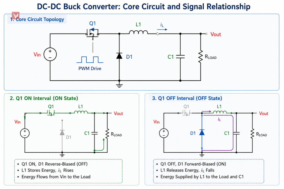
Modern converter design requires a sequence of decisions that link operating mode, component stress, control stability, PCB layout, EMI behavior, and thermal reliability into one coherent engineering process.
This guide presents that process in practical terms. It begins with topology choice and conduction mode, moves into parametric calculations for component selection, then addresses troubleshooting, layout, and thermal management so the final design is stable, manufacturable, and easier to source in real supply conditions.
Fundamental Topologies and Core Operating Mechanisms
The first design decision is whether the converter should be isolated or non-isolated. Non-isolated topologies such as buck, boost, and buck-boost are generally chosen when the input and output grounds can be shared and the priority is efficiency, simplicity, and compact size. Isolated topologies such as flyback and forward are typically used when safety isolation, noise isolation, or multiple output rails are required.
Isolated designs introduce transformer parasitics and common-mode paths that require additional control in both circuit design and layout, while non-isolated designs are structurally simpler but still demand tight management of switching nodes and current loops.
|
Topology Type
|
Common Examples
|
Typical Strengths
|
Common Trade-Offs
|
|---|---|---|---|
|
Non-isolated
|
Buck, Boost, Buck-Boost, SEPIC
|
Fewer parts, smaller size, higher efficiency in many low-to-medium power designs
|
No galvanic isolation, layout sensitivity at high switching speeds
|
|
Isolated
|
Flyback, Forward, Half-Bridge, Full-Bridge
|
Safety isolation, easier handling of large conversion ratios, multiple outputs possible
|
More complex magnetics, more parasitic paths, often higher design complexity
|
CCM VS DCM
|
Operating Mode
|
Inductor Current Behavior
|
Typical Benefit
|
Typical Cost
|
|---|---|---|---|
|
CCM
|
Current never reaches zero
|
Lower ripple current, improved output filtering, often better for medium/high load
|
Larger inductance, possible slower transient behavior
|
|
DCM
|
Current falls to zero each cycle
|
Smaller magnetics possible, useful at light load
|
Higher peak current, more stress, different small-signal behavior
|
Step-by-Step Parametric Calculations for Optimal Component Selection
Once the topology is fixed, calculation begins with operating boundaries rather than nominal values. A competent design starts from input voltage range, output voltage, output current, allowable ripple, switching frequency, ambient temperature, and efficiency target because every key component value shifts when those constraints move.
For a buck converter, the ideal duty cycle is approximated by: \(D = \frac{V_{out}}{V_{in}}\) This relation is only the first estimate, because real designs must account for MOSFET voltage drops, diode loss in asynchronous designs, dead time, and efficiency margin. Still, it establishes the switching ratio and quickly indicates whether the chosen input range is reasonable for the target output.
The inductor is usually selected from ripple current rather than from arbitrary catalog preference. A common design target is to set inductor ripple current to roughly 20% to 40% of output current in many buck designs, an approach reflected in practical design guidance for converter sizing. For a buck stage, one standard expression is: \(L = \frac{(V_{in} - V_{out}) \cdot D}{\Delta I_L * f_s}\)
- \(V_{in}\) is the input voltage.
-
\(V_{out}\) is the output voltage.
-
\(D\)
is the duty cycle.
-
\(\Delta I_L\)
is the target inductor ripple current.
-
\(f_s\)
is the switching frequency.
The output capacitor is then sized from allowable output ripple and transient demand. In simplified form, the capacitive component of ripple for a buck converter can be approximated as: \(C \ge \frac{\Delta I_L}{8 f_s \Delta V_{out}}\) But that expression is incomplete on its own, because ESR often contributes a significant additional ripple term. Practical design references consistently emphasize choosing low-ESR capacitors and accounting for DC bias and parasitics instead of treating capacitance as an ideal number on paper.
Example
A short example shows the logic. Suppose the target is 12 V input, 5 V output, 2 A load, 500 kHz switching frequency, and 30% ripple current. The ripple target is 0.6 A, the duty cycle is approximately 0.417, and the ideal inductance is about 9.7 µH, which would usually lead to a standard-value choice such as 10 µH with sufficient saturation margin. The capacitor would then be selected not only by capacitance but also by ESR, ripple-current rating, temperature class, and available package footprint.
Balancing Theoretical Parameters with Real-World Component Availability
This is the point where many otherwise solid designs meet commercial reality. The calculated inductor value may not exist as a standard stocked part in the desired current rating, the preferred low-ESR capacitor may have severe lead times, or the selected MOSFET and PMIC may disappear from franchised availability for months.
That gap between theoretical design and buildable design is where sourcing support becomes strategically important. Vigorcomp, positioned as one of the global top electronic component distributors, can be introduced here not merely as a supplier but as a practical design enabler for engineers facing shortages, allocation pressure, or urgent build schedules. Vigorcomp provides sourcing, purchasing strategy, sales and distribution support, and worldwide delivery, with a focus on electronic components and supply solutions.
-
The nearest available part often differs from the ideal calculated part value.
-
Cross-reference support can prevent a redesign when a mainstream brand part is unavailable.
-
Immediate stock visibility reduces the time lost between schematic completion and actual prototype build.
Common Design Pitfalls and Troubleshooting Power Supply Failures
Two recurring trouble sources deserve particular attention. The first is MOSFET gate charge. TI explains that the gate driver must supply the total gate charge each switching cycle, which directly affects driver demand and switching behavior. When gate charge is too high for the selected driver or switching frequency, transition times lengthen, switching loss rises, and thermal margin shrinks.
For higher-voltage or higher-power converter designs, engineers may also evaluate power semiconductor devices such as IGBTs and SiC MOSFETs, where switching speed, conduction loss, voltage capability, and thermal performance can significantly affect overall converter efficiency.
The second is diode reverse recovery, especially in non-synchronous or mixed topologies. Reverse recovery injects extra current during switching transitions, reducing efficiency and worsening noise. In high-frequency designs, it can be one of the hidden reasons why a prototype runs hotter or emits more noise than the spreadsheet predicted.
Loop instability is another major failure mode. Symptoms include output oscillation, abnormal startup behavior, poor load-step response, audible noise, or intermittent overvoltage and undervoltage events. Because CCM and DCM do not share the same small-signal behavior, compensation that appears acceptable in one operating region may be weak in another, especially near boundary conduction.
A practical troubleshooting sequence usually includes:
- Verify switching-node waveform shape and duty ratio.
- Check whether inductor current is operating in CCM, DCM, or boundary mode under actual load.
- Measure output ripple and separate capacitive ripple from ESR-induced ripple.
- Inspect compensation network values and compare transient response against expectations.
Confirm that the selected MOSFET, diode, and inductor are not approaching thermal or saturation limits.
In many cases, emergency correction involves compensation adjustment rather than full redesign. Small changes in the error amplifier RC network, together with better output capacitor selection or improved layout around the feedback path, can move a design from marginally stable to production-ready. That said, compensation should never be treated independently from layout, because feedback noise and switch-node coupling often imitate control-loop problems.
Advanced PCB Layout Guidelines for Low EMI Risk
PCB layout is part of the electrical design itself. Minimizing critical high-slew-rate current loops reduces parasitic inductance and magnetic coupling, which in turn lowers conducted and radiated EMI while also helping efficiency and cost.
The most important rule is to minimize the area of the hot loop. In a buck converter, that loop typically includes the input capacitor, the switching MOSFET path, and the return path. The smaller and tighter this loop is on the PCB, the lower the parasitic inductance and the lower the overshoot, ringing, and EMI risk.
The second rule is to control the switch node. The switch node is electrically noisy because it experiences high dv/dt, and TI identifies this node as a major common-mode noise source in non-isolated designs. (Source: Texas Instructment) The copper area of the SW node should therefore be kept as small as practical, and it should be routed away from the feedback trace, compensation network, and other sensitive low-level analog paths.
|
Layout Focus
|
Good Practice
|
Risk If Ignored
|
|---|---|---|
|
Hot loop
|
Place input capacitor close to switching devices and return path
|
Higher ringing, overshoot, conducted EMI
|
|
SW node
|
Keep copper area compact and away from feedback path
|
More capacitive coupling and radiated noise
|
|
FB routing
|
Use short, quiet routing isolated from power switching nodes
|
Ripple injection, false regulation error, instability
|
|
Grounding
|
Separate power ground and signal ground intelligently, then join appropriately
|
Ground bounce, noisy feedback reference, measurement confusion
|
|
Thermal vias
|
Use beneath exposed pads or heat-spreading copper where applicable
|
Higher junction temperature, weaker reliability margin
|
Ground strategy also matters. A continuous low-impedance return path helps suppress noise, but power ground and signal ground should still be arranged deliberately so that sensitive control signals do not share noisy return current paths with the power stage. In practice, designers often use a quiet analog reference region and a separate high-current power return region, then connect them in a controlled way near the regulator reference point.
For isolated converters, the layout challenge broadens because transformer parasitics and primary-secondary coupling contribute to common-mode noise. TI’s EMI guidance discusses common-mode behavior in isolated designs and shows that asymmetry and parasitic capacitance can strongly shape EMI results, which is why transformer placement, Y-capacitor decisions, and grounding structure must be treated as first-order layout choices, not afterthoughts.
Managing Thermal Dissipation and Reliability for Long Lifetime
A converter that passes the first prototype test is not necessarily ready for field service. Long-term reliability depends on controlling conduction loss, switching loss, magnetic loss, capacitor stress, and temperature rise across the whole assembly. Even excellent electrical performance can degrade quickly when thermal design is treated as secondary.
At a simplified level, MOSFET conduction loss scales with \(I^2 R_{DS(on)}\) while switching loss increases with voltage, current, switching frequency, and transition time. This is why higher frequency can reduce passive size but increase power loss and EMI pressure at the same time. TI’s EMI material directly connects faster switching edges with higher dv/dt and di/dt, underscoring the familiar trade-off between compactness, efficiency, and noise.
Several thermal practices consistently improve reliability:
- Use adequate copper area to spread heat from switching devices and magnetics.
- Add thermal vias beneath exposed pads or heat-dense regions to move heat into inner or backside copper.
- Keep high-loss parts away from sensitive references and electrolytic capacitors where possible.
- Leave temperature margin rather than designing to absolute maximum ratings.
For industrial and automotive applications especially, stable operation across temperature and supply variation is often a more valuable success metric than headline efficiency at one nominal condition.
Practical Design Checklist
A concise checklist helps unify the entire design process:
- Confirm whether isolation is functionally or regulatorily required before topology selection.
- Choose CCM or DCM deliberately based on load range, ripple targets, and control complexity.
- Calculate duty cycle, inductance, ripple current, and output capacitance from worst-case operating conditions rather than nominal conditions.
- Validate real component availability before freezing schematic values, especially for PMICs, MOSFETs, inductors, and low-ESR capacitors.
Treat troubleshooting, compensation, layout, EMI control, and thermal performance as linked design tasks rather than separate cleanup steps.
Conclusion
A well-executed DC-DC converter circuit is rarely the result of one perfect equation. It is more often the result of disciplined iteration across topology, operating mode, component selection, sourcing practicality, loop behavior, layout, and thermal control. That is also why a distributor with global sourcing reach and cross-reference capability can contribute meaningfully to the design cycle: the electrical solution only becomes useful when it can actually be built, tested, and scaled.