
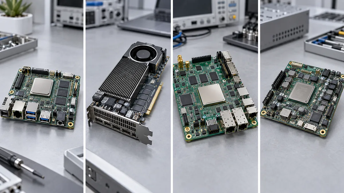
A workload that performs well on one architecture may behave very differently on another. The reason is rarely just clock speed or core count. In real systems, the limiting factor may be branch behavior, memory bandwidth, host-device transfers, I/O timing, data movement, or the structure of the algorithm itself.
A CPU may handle irregular control flow efficiently but lose time to cache misses or scheduling. A GPU may offer very high throughput yet be less efficient for small or highly irregular workloads. An FPGA can implement deterministic hardware pipelines but requires more specialized engineering. An ASIC can remove much of the overhead of programmability, although its function is largely fixed once manufactured.
The useful design question is therefore not “Which is fastest?” but which architecture best matches the workload, latency target, development model, production volume, and expected product lifetime.
Key Takeaways
- CPU: Best suited to general-purpose software, complex control flow, operating systems, and applications that change frequently.
- GPU: Well suited to large parallel workloads such as AI training, graphics, simulation, and matrix-heavy numerical computation.
- FPGA: Useful for deterministic data paths, streaming processing, protocol handling, custom I/O, and real-time workloads.
- ASIC: Most relevant when a function is stable enough to justify dedicated silicon and the expected production economics support the additional development effort.
- Heterogeneous systems are common. A CPU, GPU, FPGA, and ASIC may serve different roles in the same product.
The distinction between these devices is primarily architectural. A CPU and GPU expose largely fixed processing structures and change behavior through software. An FPGA uses configurable logic, routing, memory, and hard IP to create application-specific hardware. An ASIC implements the required circuitry permanently during fabrication.
That difference affects not only performance, but also how a system is programmed, verified, updated, manufactured, and supported over its lifecycle.
FPGA vs CPU vs GPU vs ASIC Comparison
| Factor | CPU | GPU | FPGA | ASIC |
| Core Model | General-purpose cores | Parallel compute units | Configurable hardware | Fixed custom hardware |
| Best Fit | Software and control | Parallel computation | Streaming and real-time logic | Stable specialized functions |
| Latency | Workload-dependent | Often throughput-oriented | Can be deterministic | Can be tightly optimized |
| Parallelism | Threads and vectors | Massive data parallelism | Spatial and pipelined | Fixed hardware parallelism |
| Reconfigurable | Software only | Software only | Yes | No |
| Development | Software | Parallel software | HDL/HLS and hardware design | Full silicon design flow |
| Upfront Cost | Relatively low | Relatively low | Higher engineering effort | High NRE |
| Volume Economics | Device cost remains | Device cost remains | FPGA cost remains | Can improve at scale |
These comparisons are useful only when tied to a specific workload. Latency, throughput, power, and cost can vary substantially depending on memory traffic, interfaces, software stack, process technology, utilization, and implementation quality.
A CPU can outperform an accelerator when the workload contains unpredictable branches or frequent software changes. A GPU can dominate a highly parallel numerical workload. An FPGA may be more suitable when processing must follow a fixed data path with predictable timing. An ASIC becomes more attractive when the function is mature enough to justify custom silicon.
Why These Four Architectures Behave So Differently
- A CPU is built to execute many types of software efficiently. Modern processors combine general-purpose cores with caches, branch prediction, instruction scheduling, memory management, and other mechanisms designed to handle irregular workloads.
- A GPU allocates much more silicon to parallel arithmetic. In the NVIDIA CUDA programming model, many threads execute across groups of streaming multiprocessors. This works particularly well when similar operations can be applied repeatedly to large datasets.
- An FPGA takes a different approach. Instead of mapping software instructions onto fixed processor cores, the designer configures programmable hardware resources into an application-specific circuit. Typical FPGA resources include LUTs, registers, DSP blocks, embedded memory, programmable routing, and device-dependent hard IP. Intel's FPGA architecture documentation describes this as a spatial form of computation.
- An ASIC is also application-specific hardware, but the implementation is fixed during fabrication. Removing programmable routing and configuration structures gives the designer more freedom to optimize area, power, interfaces, and data paths. The trade-off is reduced flexibility after manufacturing.
How Performance Differs In Real Workloads
Performance depends on where the bottleneck occurs.
- A CPU workload may be limited by cache misses, memory latency, or branch behavior.
- A GPU application may be limited by host-device transfers, synchronization, or insufficient parallelism.
- An FPGA design may be limited by timing closure, memory interfaces, transceivers, or pipeline structure.
- An ASIC may remove some of these constraints but introduces a very different development model.
Latency And Determinism
- CPU response times can be very short, but operating-system scheduling, interrupts, cache state, and memory access can introduce variability.
- GPUs are often optimized for throughput. Kernel launches, batching, synchronization, and movement between CPU and GPU memory may matter when the workload is small or latency-sensitive.
- FPGAs can create fixed-depth pipelines in which data begins processing as soon as it arrives. That can produce predictable timing, although actual latency still depends on pipeline depth, clock frequency, buffering, memory access, and interface design.
Throughput And Data Movement
GPUs are particularly effective when large amounts of arithmetic can be performed in parallel. FPGAs instead exploit spatial and pipeline parallelism.
In many systems, however, memory movement matters more than theoretical arithmetic capability. The best architecture is often the one that keeps data moving efficiently through the required processing stages.
Development Complexity, Cost, And Time To Market
- CPU development is usually closest to conventional software engineering. Mature compilers, operating systems, libraries, and debugging tools allow functionality to change without redesigning the hardware.
- GPU development remains software-oriented but requires a parallel programming model. Frameworks such as CUDA and higher-level AI libraries can reduce implementation effort for workloads that already map well to GPU hardware.
- FPGA development crosses into digital hardware engineering. A typical project may involve RTL or HLS design, simulation, synthesis, placement and routing, timing analysis, and hardware verification. The PCB may also require multiple power rails, high-speed memory routing, clocking, configuration circuitry, and controlled-impedance serial interfaces.
- ASIC development extends this process into physical silicon implementation. Verification, design-for-test, clock-tree synthesis, power analysis, timing signoff, masks, fabrication, packaging, and production test all become part of the project.
The development model can therefore influence architecture selection as strongly as performance. A technically attractive accelerator may still be unsuitable if the project cannot support the required verification effort, design expertise, or development schedule.
How Economics Change From Prototype To Mass Production
The economic relationship between FPGA and ASIC is more complex than the common rule that FPGAs suit low volume and ASICs suit high volume.
An FPGA is purchased as a finished programmable component. This avoids mask costs and much of the manufacturing investment associated with custom silicon, while also allowing changes after the hardware has been built.
An ASIC requires substantial non-recurring engineering before production begins. Costs may include architecture work, IP licensing, verification, physical design, masks, qualification, packaging, and test development.
At sufficient scale, an ASIC may provide better per-unit economics because it does not need to carry the programmable routing and general-purpose resources of an FPGA. The crossover point, however, depends on many variables:
- Process node and die size
- Package and manufacturing yield
- Verification and qualification expense
- Total lifetime production volume
- FPGA and supporting-system cost
Requirements stability matters as well. If interfaces, algorithms, or standards are still changing, the ability to reconfigure an FPGA may have significant economic value even when the FPGA itself costs more per unit.
Choosing The Right Architecture For Common Applications
Different workloads favor different combinations of flexibility, throughput, latency, and specialization.
| Application | Common Architecture Pattern | Main Constraint |
| AI Training | CPU + GPU | Parallel compute throughput |
| Edge AI | CPU/GPU/FPGA/ASIC | Power, latency, model size |
| High-Frequency Trading | CPU + FPGA | Deterministic data paths |
| Networking | CPU + FPGA or ASIC | Packet processing and I/O |
| Machine Vision | CPU + GPU or FPGA | Image throughput and latency |
| Industrial Control | CPU/MCU + FPGA | Timing and I/O determinism |
| Automotive | Heterogeneous systems | Sensing, compute, networking |
| Video Processing | GPU, FPGA, or ASIC | Throughput and codec support |
| Telecom | CPU + FPGA/ASIC | Signal processing and protocols |
| Instrumentation | CPU + FPGA | Acquisition and real-time processing |
AI illustrates the trade-off well. GPUs are widely used for large matrix workloads, while FPGAs can be useful when inference must be closely integrated with custom data flow or I/O. ASIC-based accelerators provide still greater specialization.
Networking shows a different pattern. CPU software may manage configuration and control, while an FPGA or ASIC handles high-speed packet processing.
The application should therefore define the architecture, not the other way around.
Why Real Systems Often Combine CPU, GPU, FPGA, And ASIC
Many practical systems are heterogeneous because different tasks have different computational characteristics.
A CPU may run the operating system, configuration software, protocol stacks, and high-level decision logic. A GPU may accelerate numerically intensive workloads. An FPGA can handle deterministic preprocessing or high-speed I/O, while an ASIC may implement a mature fixed function.
A simplified architecture might look like this:
Network Or Sensor Input
          ↓
     FPGA Or ASIC
   Real-Time Processing
          ↓
         CPU
 Control And Coordination
          ↓
         GPU
 Parallel Compute Or AI
The order can vary widely.
A SmartNIC may process packets before data reaches the host CPU. An industrial controller may use programmable logic for precise I/O timing while a processor handles communications. An AI appliance may use CPUs for orchestration and GPUs for model execution.
Integrated platforms blur these boundaries further. AMD Versal adaptive SoCs, for example, combine processor cores, programmable logic, DSP resources, and hardened interfaces.
For system architects, the more useful question is often not which architecture should run the entire application, but which functions belong on each one.
What Matters When Selecting An FPGA
Once an FPGA has been selected at the architecture level, device selection moves to a more detailed set of constraints.
Logic capacity matters, but comparing devices only by LUT or logic-cell count can be misleading because FPGA families use different internal architectures and counting methods.
Several resources usually deserve closer attention:
- DSP blocks: Important for filtering, multiplication, MAC operations, and other arithmetic-heavy pipelines.
- On-chip memory: BRAM, distributed RAM, or larger embedded memories may reduce dependence on external DRAM.
- External memory interfaces: DDR, LPDDR, or HBM support can determine achievable system bandwidth.
- High-speed transceivers: Relevant to Ethernet, PCI Express, optical links, and converter interfaces.
- Package and I/O: Package choice affects available pins, transceivers, thermals, and PCB complexity.
Power and temperature grade also matter. Large devices may require multiple supply rails and careful sequencing. Commercial, industrial, and automotive variants can also use different ordering codes.
For vendor-level context, the related articles Which Companies Make FPGAs? and Xilinx vs Altera vs Lattice can be used to compare supplier portfolios before narrowing the choice to individual families and part numbers.
What The Architecture Choice Means For The BOM
The processing device is only one part of a complete hardware platform.
| Architecture | Common Supporting Components |
| CPU | DRAM, storage, PMICs, clocking, network and interface ICs |
| GPU | Host CPU, PCIe, power delivery, memory, thermal hardware |
| FPGA | Flash, DDR/HBM, regulators, clocking, PHYs, optical interfaces |
| ASIC | Power, clocking, memory, interface ICs, protection devices |
An FPGA system may require external configuration memory, several regulated power rails, clock generators, and high-speed interface components. Networking-oriented FPGA boards may also need Ethernet PHYs, optical cages, jitter cleaners, and interface protection.
A GPU-based architecture can place greater emphasis on high-current power delivery, PCIe connectivity, memory bandwidth, and thermal management.
ASIC integration can reduce the number of discrete devices if functions are brought onto the custom chip, although external memory, power, analog, protection, and communication devices may still be required.
This is why the purchase price of the main processor does not represent total system cost. PCB complexity, thermal design, memory architecture, power conversion, interfaces, and software or firmware effort can materially change the economics of the final design.
Availability, Lifecycle, And Supply Chain Considerations
A technically suitable device may still be a poor fit if its lifecycle does not match the intended product.
This becomes particularly important in industrial, medical, infrastructure, transportation, and communications equipment, where products may remain in production for many years.
Key issues include product status, package availability, temperature grade, and migration effort.
Semiconductor manufacturers eventually discontinue specific ordering codes or device families. Formal Product Discontinuance Notifications normally identify affected parts, last-order dates, and related lifecycle information.
Package choice can also become a long-term constraint. A device may exist in several packages, but the design may depend on one specific option because of transceiver count, I/O allocation, thermal characteristics, or board routing.
Grade matters as well. Commercial, industrial, automotive, and extended-temperature devices may use different part numbers and may not be available across every package or speed grade.
Migration should also be considered early. Moving between FPGA families can affect pinout, IP blocks, memory interfaces, timing, and transceivers. Lifecycle planning is therefore part of architecture selection, not only a response to end-of-life notices.
A Practical Selection Framework
A CPU is usually the natural starting point when the workload is dominated by general software, complex control flow, operating-system services, and features that are expected to change frequently.
A GPU becomes more attractive when a large portion of the workload can be expressed as parallel numerical computation and existing software frameworks can make effective use of the hardware.
An FPGA deserves consideration when the system needs configurable hardware behavior, deterministic pipelines, specialized I/O, protocol processing, or tightly controlled data movement.
An ASIC becomes relevant when the function is stable enough to commit to silicon and the expected product volume, power target, integration requirements, or physical constraints can justify the additional design effort.
These choices are often combined rather than treated as exclusive alternatives.
A CPU may remain the system controller while an FPGA handles packet processing. A GPU may accelerate matrix computation while the CPU manages orchestration. An ASIC may implement a fixed high-volume function while programmable processors handle everything that still changes.
Frequently Asked Questions
What Is The Difference Between An FPGA And An ASIC?
An FPGA provides programmable logic and routing that can be reconfigured after manufacturing.
An ASIC implements fixed circuitry during fabrication.
The FPGA offers post-manufacturing flexibility, while the ASIC provides more freedom to optimize silicon for a stable function.
Can An FPGA Replace A CPU?
It can replace selected functions, but many systems still need a processor.
Some FPGAs integrate hardened processor cores or support soft processors, but CPU and FPGA resources are often used together rather than as complete substitutes.
Can A GPU Replace An FPGA?
Sometimes. If the workload is dominated by parallel arithmetic, a GPU may be the better fit. If the system depends on deterministic timing, custom interfaces, or configurable hardware pipelines, the FPGA may serve a different role.
Are FPGAs More Power Efficient Than GPUs?
They can be for certain workloads, but there is no universal rule. Efficiency depends on utilization, memory traffic, clock frequency, transceiver activity, process technology, and algorithm structure.