
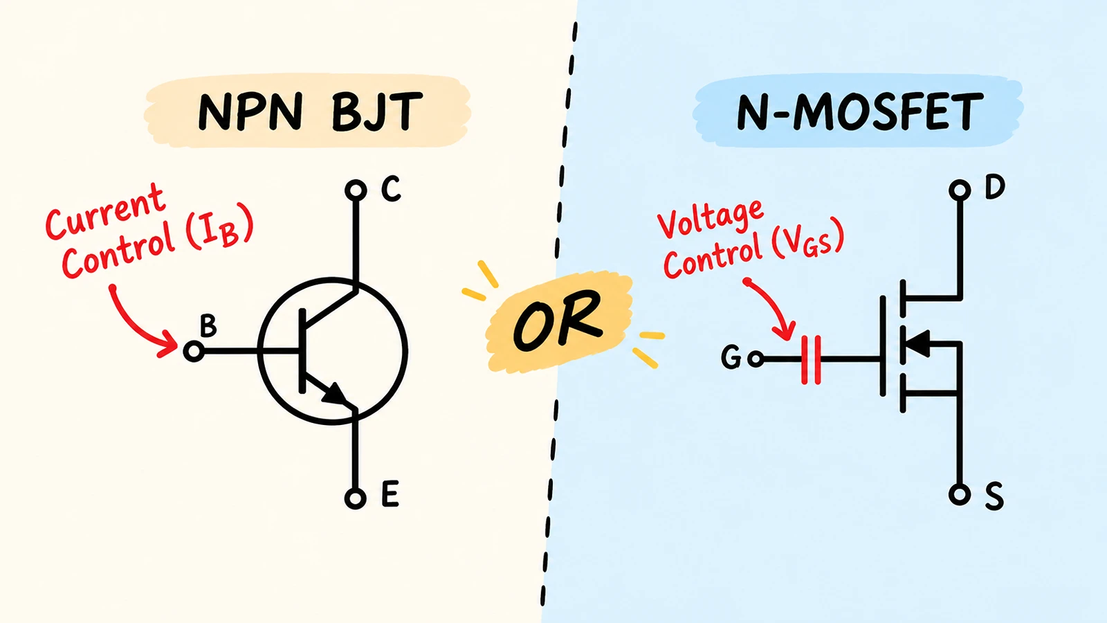
Strictly speaking, a MOSFET (Metal-Oxide-Semiconductor Field-Effect Transistor) is already a subset of the transistor family. However, in everyday circuit design and BOM sourcing, engineers and technicians asking whether to use a MOSFET or transistor are almost always comparing a MOSFET against a traditional BJT (Bipolar Junction Transistor), such as a standard NPN or PNP device. The core physical difference lies in their control mechanism: a BJT is a current-controlled device that requires continuous base current ( \(I_B\)) to stay on, whereas a MOSFET is a voltage-controlled device regulated by an insulated gate voltage ( \(V_{GS}\)) with near-zero steady-state gate current. For high-frequency PWM switching, high-current power conversion, and efficient 3.3V or 5V microcontroller load driving, the MOSFET is the primary choice; for low-noise analog amplification, ultra-low-voltage circuits operating below 1.5V, or ultra-low-cost indicator switching, the BJT remains highly effective.
Is a MOSFET a Transistor?
Yes—every MOSFET is a transistor, though not every transistor is a MOSFET. In semiconductor taxonomy, transistor is the umbrella term for any three-terminal active component used to amplify or switch electrical signals and power.
Because bipolar transistors were invented first (in 1947) and dominated discrete electronics for decades, legacy schematics, repair manuals, and component catalogs often shorthand "BJT" simply as "transistor." When you see a forum thread or design spec debating "MOSFET or transistor," it is contrasting two distinct branches of the transistor family tree:
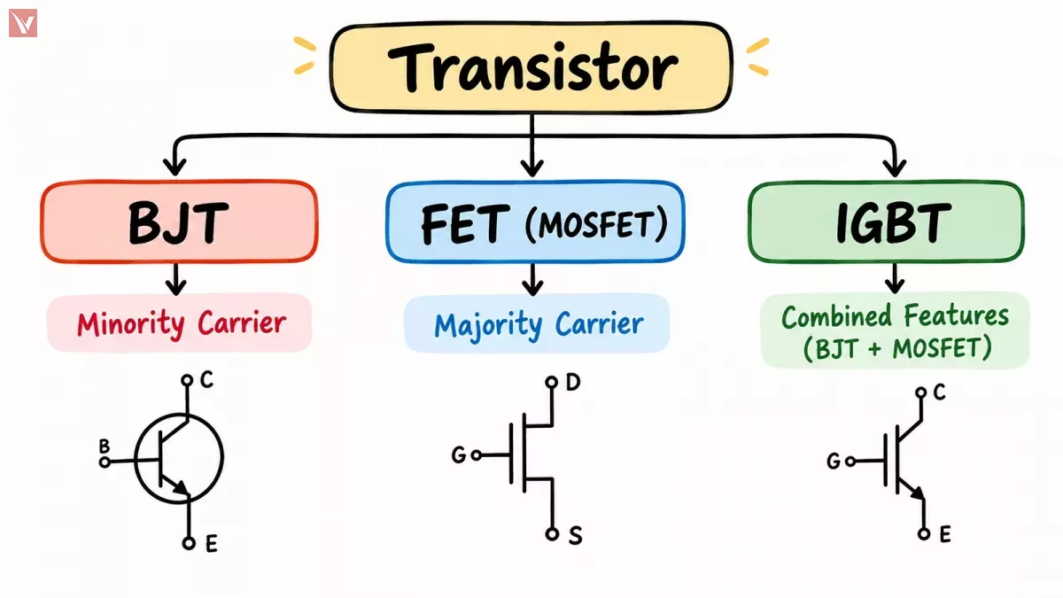
- BJT (Bipolar Junction Transistor): Uses both electrons and holes as charge carriers (hence "bipolar"). Current flowing from the Base (B) to the Emitter (E) controls a larger current flowing from the Collector (C) to the Emitter.
- MOSFET (Metal-Oxide-Semiconductor Field-Effect Transistor): A unipolar device that relies on an electric field across a thin silicon dioxide insulating layer to create a conductive channel between the Drain (D) and Source (S), controlled by the Gate (G). While discrete power MOSFETs handle board-level switching, pairing complementary N-channel and P-channel MOSFETs on a silicon die forms the foundation of digital integrated circuits—a distinction covered in our CMOS vs. MOSFET comparison.
- IGBT (Insulated-Gate Bipolar Transistor): A hybrid power switch that combines the high-input-impedance voltage gate of a MOSFET with the low high-voltage conduction loss of a BJT.
If you are inspecting a circuit diagram and need to verify whether a symbol represents an NPN/PNP BJT or an N-channel/P-channel MOSFET, refer to our electrical schematic symbols chart to check the emitter arrow and insulated gate lines.
What Is the Function of the Power Transistor or MOSFET?
The primary function of a power transistor or MOSFET is to act as a high-efficiency electronic switch or power amplifier that uses a small, low-power control signal (current or voltage) to regulate large load currents and high voltages in power supplies, motor drives, and inverters.
Electronic Power Switching
In switching applications—such as DC-DC buck/boost converters, brushed and brushless DC (BLDC) motor drives, solenoid actuators, and PWM LED dimmers—the transistor operates like a high-speed digital relay. It transitions rapidly between two states:
- Cutoff (OFF state): Blocking voltage with minimal leakage current.
- Saturation / Ohmic region (ON state): Conducting full load current with the lowest possible voltage drop across the terminals to minimize heat generation.
Signal and Power Amplification
When biased in its linear (or active) region rather than fully on or off, a power transistor or MOSFET functions as a variable resistor or controlled current source. Small fluctuations at the Base or Gate produce proportional variations in Collector or Drain current. This linear function is essential for Class A and Class AB audio power amplifiers, RF transmitters, and the pass elements inside linear voltage regulators (LDOs).
Freewheeling and Reverse Conduction
Unlike a standard BJT, a discrete power MOSFET contains an intrinsic parasitic component resulting from its vertical semiconductor structure: an internal body diode (integral reverse P-N junction diode) connected from Source to Drain (in an N-channel device).
- In inductive load switching—such as H-bridge motor drivers or synchronous buck converters—this body diode provides a critical freewheeling path for reverse inductive currents during switching dead-times.
- Additionally, rugged power MOSFETs are specified with an Unclamped Inductive Switching (UIS) or single-pulse avalanche energy rating ( \(E_{AS}\) ), allowing them to absorb brief high-voltage inductive kickback spikes without immediate destruction.
Small-Signal vs. Power Transistors
In manufacturer classification standards (such as ROHM and Toshiba engineering guidelines), the boundary between a small-signal transistor and a power transistor is generally set at a maximum power dissipation ( \(P_D\) or \(P_{tot}\)) of 1 Watt:
- Small-Signal Transistors ( \(P_D\) less than 1 W): Typically housed in compact surface-mount packages like SOT-23, SOT-323, or through-hole TO-92, used for logic level shifting, indicator LED driving, and pre-amplification.
- Power Transistors ( \(P_D\) of 1 W or greater): Housed in thermally enhanced packages with metal tabs or exposed pads—such as TO-220, TO-247, DPAK (TO-252), D2PAK, or thermally enhanced SO-8—designed to transfer heat into a PCB copper pour or external heatsink.
MOSFET vs. Transistor (BJT)
When deciding between a MOSFET and a BJT for a specific circuit node, four electrical mechanisms dictate performance: input drive power, on-state conduction loss, switching speed, and low-voltage/ESD behavior.
| Feature / Parameter | BJT (Bipolar Junction Transistor) | MOSFET (Metal-Oxide-Semiconductor FET) | IGBT (Insulated-Gate Bipolar Transistor) |
|---|---|---|---|
| Terminal Names | Base (B), Collector (C), Emitter (E) | Gate (G), Drain (D), Source (S) | Gate (G), Collector (C), Emitter (E) |
| Control Mechanism | Current-driven (requires continuous Base current IB) | Voltage-driven (regulated by Gate-Source voltage VGS) | Voltage-driven (regulated by Gate-Emitter voltage VGE) |
| Input Impedance & Steady-State Drive | Low input impedance; consumes continuous drive power while ON | Very high capacitive input impedance; near-zero DC gate current in steady state | High capacitive input impedance; near-zero DC gate current in steady state |
| On-State Loss Behavior | Scales linearly with current: P = IC × VCE(sat) | Scales quadratically with current: P = ID2 × RDS(on) | Low saturation voltage drop even at blocking voltages above 600 V |
| Intrinsic Body Diode | None (blocks reverse current up to VEBO limit unless co-packaged) | Yes (integral Source-to-Drain P-N junction diode conducts in reverse) | None intrinsic (often co-packaged with an external anti-parallel fast recovery diode) |
| Typical Switching Speed | Medium to slow (limited by minority carrier storage time ts; typically under 25–50 kHz in power stages) | Very fast (majority carrier device; nanosecond transitions from 50 kHz up to several MHz) | Medium (limited by collector tail current during turn-off; typically under 30–50 kHz) |
| Minimum Turn-On Control Voltage | Approx. 0.6 V to 0.7 V (VBE forward diode drop for silicon) | VGS(th) is typically 1.0 V to 4.0 V; requires 2.5 V to 10 V for full low-resistance saturation | Typically requires 15 V gate drive for full saturation |
| Parallel Operation Thermal Stability | Negative temperature coefficient (prone to current hogging and thermal runaway without emitter ballast resistors) | Positive RDS(on) temperature coefficient (channels naturally balance current when paralleled) | Requires closely matched devices and symmetrical thermal layout |
Voltage Control vs. Current Control
A silicon BJT's Base-Emitter junction behaves like a forward-biased diode ( \(V_{BE} \approx 0.7\text{ V}\)). Its Collector current ( \(I_C\)) is governed by its DC current gain ( \(h_{FE}\) or \(\beta\)): \(I_B = \frac{I_C}{h_{FE}}\) In power BJTs operating in deep saturation, effective \(\) often drops to between 10 and 25. Driving a \(5\text{ A}\) load with a power BJT can therefore demand \(250\text{ mA}\) to \(500\text{ mA}\) of continuous Base current—far more than a microcontroller GPIO pin (typically rated for \(8\text{ mA}\) to \(20\text{ mA}\)) can supply directly.
A MOSFET isolates the Gate from the conductive channel using a thin oxide layer. Once the Gate capacitance is charged to the desired \(V_{GS}\) voltage, steady-state DC gate leakage current ( \(I_{GSS}\)) is measured in nanoamperes ( \(\text{nA}\)).
Conduction Loss Math
The most critical thermal decision between a power BJT and a power MOSFET comes down to how they dissipate heat when fully turned on:
- MOSFET Conduction Loss (Ohmic Behavior): When fully enhanced, a MOSFET acts like a resistor with an on-state resistance of \(R_{DS(on)}\) . Its conduction power loss is proportional to the square of the drain current:
- BJT Conduction Loss (Saturation Voltage Behavior): A saturated BJT exhibits a relatively fixed Collector-Emitter voltage drop, \(V_{CE(\text{sat})}\) , plus the power consumed by the Base drive:
What the math means for your circuit:
In low-to-medium voltage systems (under \(200\text{ V}\)), modern trench MOSFETs achieve \(R_{DS(\text{on})}\) values as low as a few milliohms ( \(\text{m}\Omega\)). At \(R_{DS(\text{on})} = 10\text{ m}\Omega\), a MOSFET with \(P = 5^2 \times 0.010\,\Omega = 0.25\text{ W}\) dissipates just: \(V_{CE(\text{sat})} = 1.0\text{ V}\) By contrast, a power BJT with \(V_{CE(\text{sat})}\) at \(5\text{ A}\) dissipates at least \(5\text{ W}\), requiring a bulky heatsink. Furthermore, because MOSFET \(R_{DS(\text{on})}\) has a positive temperature coefficient (resistance increases as the die heats up), multiple MOSFETs can be wired in parallel to share heavy currents safely. BJTs exhibit a negative temperature coefficient for \(V_{CE(\text{sat})}\), meaning the hottest BJT draws more current, leading to thermal runaway and secondary breakdown unless emitter ballast resistors are added.
However, as blocking voltage ratings climb above \(600\text{ V}\), the thicker silicon drift region required in a standard silicon MOSFET causes \(R_{DS(\text{on})}\) to rise sharply. Under combined high voltage and high current, \(I_D^2 \times R_{DS(\text{on})}\) eventually exceeds the linear \(I_C \times V_{CE(\text{sat})}\) loss of bipolar conductivity modulation—which is why high-voltage industrial drives shift to IGBTs or wide-bandgap Silicon Carbide (SiC) MOSFETs.
Switching Speed
Because a MOSFET is a majority carrier device, current flow stops as soon as the electric field at the Gate collapses. Its switching speed is limited primarily by how fast the external gate driver circuit can charge and discharge the total gate charge ( \(Q_g\)) and input capacitance ( \(C_{iss}\)): \(I_{\text{gate(avg)}} = Q_g \times f_{\text{sw}}\) A BJT is a minority carrier device. Driving it into saturation floods the base region with excess minority carriers. When the Base drive is removed, the transistor cannot turn off until those stored charges recombine or are swept out—a delay known as storage time ( \(t_s\)). This storage delay creates significant crossover switching loss, restricting power BJTs to lower switching frequencies (typically below \(25\text{ kHz}\) to \(50\text{ kHz}\)), whereas MOSFETs easily switch from \(100\text{ kHz}\) into the megahertz range.
Ultra-Low-Voltage Operation and ESD Ruggedness
Despite the dominance of MOSFETs in power switching, BJTs hold two distinct hardware advantages:
- Sub-1.8V Operation: A silicon BJT reliably turns on at \(V_{BE} \approx 0.65\text{ V}\) to \(0.7\text{ V}\) . If you are designing a circuit powered by a single \(1.2\text{ V}\) NiMH cell or a \(1.5\text{ V}\) alkaline battery, standard MOSFETs—and even many logic-level MOSFETs—will fail to turn on fully because their gate threshold voltage ( \(V_{GS(\text{th})}\) ) is too high.
- Electrostatic Discharge (ESD) Tolerance: The ultra-thin gate oxide of a MOSFET can rupture permanently if exposed to voltage spikes exceeding its maximum \(V_{GS}\) rating (often \(\pm 12\text{ V}\) to \(\pm 20\text{ V}\) ) or minor ESD events below \(100\text{ V}\) (Human Body Model). Standard BJTs consist of rugged P-N junctions that tolerate transient voltage spikes far better without extra gate-clamping Zener diodes.
Real-World Datasheet Showdown
To see how these physical principles translate into real component selection, the table below compares verified manufacturer datasheet parameters across two standard industry footprints: SOT-23 (small-signal / compact surface-mount switching) and TO-220 (through-hole power switching).
| Part Number & Manufacturer | Transistor Type & Package | Max Voltage (VCEO or VDSS) | Max Continuous Current (IC or ID @ 25°C) | On-State Loss Metric (Max Value @ Test Conditions) | Control / Threshold Spec | Primary Engineering Use Case |
|---|---|---|---|---|---|---|
| MMBT3904 (Nexperia) |
NPN BJT (SOT-23) |
40 V | 200 mA | VCE(sat) = 0.2 V max (@ IC = 10 mA, IB = 1 mA) VCE(sat) = 0.3 V max (@ IC = 50 mA, IB = 5 mA) |
VBE ≈ 0.65 V–0.85 V hFE ≥ 100 (@ 10 mA, 1 V) |
Ultra-low-cost general-purpose signal amplification, LED indicator switching, and low-voltage logic inversion |
| 2N7002 (Nexperia) |
N-Channel Trench MOSFET (SOT-23) |
60 V | 300 mA | RDS(on) = 5.3 Ω max (@ VGS = 4.5 V, ID = 0.05 A) RDS(on) = 5.0 Ω max (@ VGS = 10 V, ID = 0.5 A) |
VGS(th) = 1.0 V to 2.5 V VGS(max) = ±20 V |
Zero-DC-gate-current logic level shifting, 5V/12V small relay coil driving, and open-drain bus interfacing |
| IRLML6344TRPbF (Infineon) |
N-Channel Logic-Level Power MOSFET (SOT-23 / Micro3) |
30 V | 5.0 A | RDS(on) = 29 mΩ max (@ VGS = 4.5 V, ID = 5.0 A) RDS(on) = 37 mΩ max (@ VGS = 2.5 V, ID = 4.0 A) |
VGS(th) = 0.5 V to 1.1 V VGS(max) = ±12 V |
Direct 3.3V/5V MCU load switching up to several amps in space-constrained SMD boards with minimal heat |
| TIP31C (onsemi) |
NPN Silicon Power BJT (TO-220AB) |
100 V | 3.0 A | VCE(sat) = 1.2 V max (@ IC = 3.0 A, IB = 375 mA) | VBE(on) = 1.8 V max (@ 3 A) hFE = 10 to 50 (@ 3 A, 4 V) |
Legacy linear power regulators, audio amplifier output stages, and medium-voltage switching up to 100 V |
| IRLZ44NPbF (Infineon) |
N-Channel Logic-Level Power MOSFET (TO-220AB) |
55 V | 47 A | RDS(on) = 22 mΩ max (@ VGS = 10 V, ID = 25 A) RDS(on) = 25 mΩ max (@ VGS = 5.0 V, ID = 25 A) RDS(on) = 35 mΩ max (@ VGS = 4.0 V, ID = 21 A) |
VGS(th) = 1.0 V to 2.0 V VGS(max) = ±16 V |
High-current 5V MCU motor drives, DC-DC converters, and heavy resistive heaters under 55 V |
Small-Signal SMD Switch Comparison
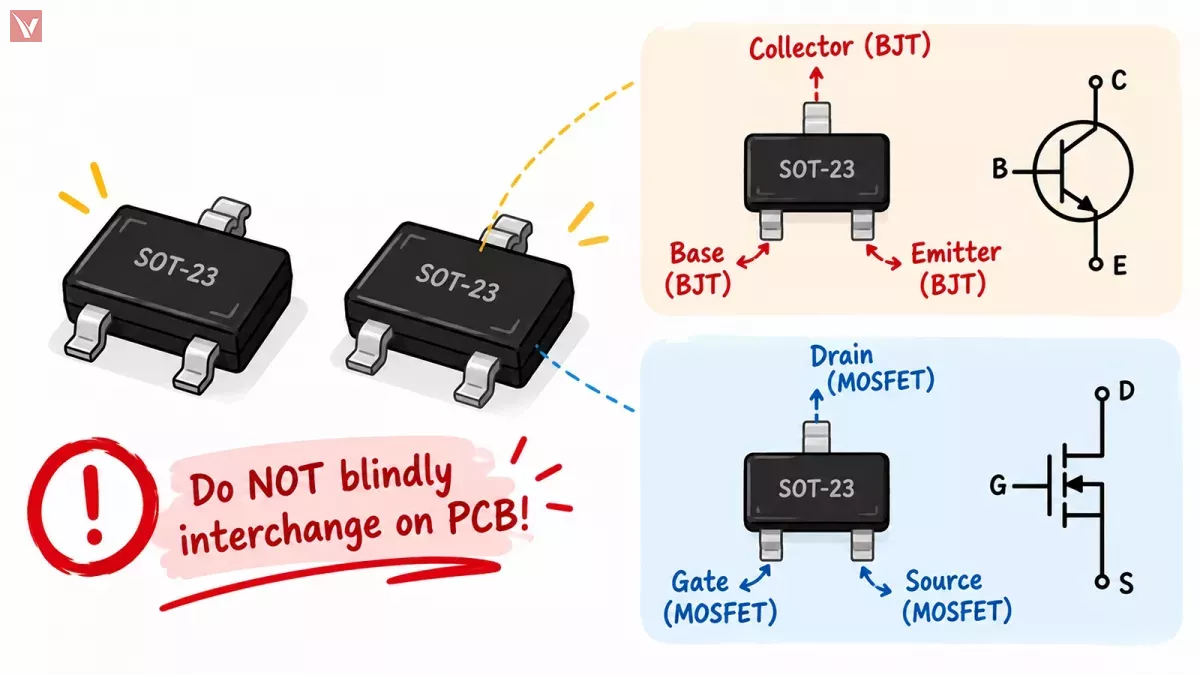
In the ubiquitous 3-pin SOT-23 package, engineers frequently choose between the MMBT3904 (NPN BJT), the 2N7002 (standard small-signal N-MOSFET), and modern trench MOSFETs like the IRLML6344TRPbF:
- If you are switching \(20\text{ mA}\) for an status LED from a \(3.3\text{ V}\) GPIO, the MMBT3904 costs fractions of a cent and works reliably with a simple \(1\text{ k}\Omega\) to \(4.7\text{ k}\Omega\) series base resistor.
- The classic 2N7002 eliminates continuous base current draw and blocks up to \(60\text{ V}\) , but its maximum \(R_{DS(\text{on})}\) of \(5.3\,\Omega\) at \(V_{GS} = 4.5\text{ V}\) causes noticeable voltage drop if load current exceeds \(100\text{ mA}\) .
- By contrast, Infineon's IRLML6344TRPbF demonstrates how far low-voltage MOSFET technology has advanced: housed in the exact same SOT-23 footprint, it specifies a maximum \(R_{DS(\text{on})}\) of just \(29\text{ m}\Omega\) at \(V_{GS} = 4.5\text{ V}\) (and \(37\text{ m}\Omega\) at \(V_{GS} = 2.5\text{ V}\) ), allowing a tiny SMD transistor to switch \(3\text{ A}\) to \(4\text{ A}\) directly from a \(3.3\text{ V}\) microcontroller pin without overheating. (Note its tighter \(\pm 12\text{ V}\) maximum gate voltage rating.)
Through-Hole Power Switch Comparison
Comparing two industry-standard TO-220 devices—the onsemi TIP31C (NPN Power BJT) and the Infineon IRLZ44NPbF (Logic-Level Power MOSFET)—highlights the dramatic thermal difference at a 3.0 A load current:
- TIP31C Thermal Dissipation at 3.0 A:
- According to the onsemi datasheet, saturating the TIP31C at \(I_C = 3.0\text{ A}\) requires a massive Base current of \(I_B = 375\text{ mA}\) and results in a maximum saturation drop of \(V_{CE(\text{sat})} = 1.2\text{ V}\) (with \(V_{BE(\text{on})}\) up to \(1.8\text{ V}\) ). Total worst-case power dissipation inside the package is:
At \(4.28\text{ W}\), a bare TO-220 package (typical junction-to-ambient thermal resistance \(R_{\theta JA} \approx 62.5^\circ\text{C/W}\)) would exceed its \(150^\circ\text{C}\) maximum junction temperature in seconds without a metal heatsink.
- IRLZ44NPbF Thermal Dissipation at 3.0 A:
- Driven directly by a \(5.0\text{ V}\) logic signal, the IRLZ44NPbF guarantees a maximum \(R_{DS(\text{on})}\) of \(0.025\,\Omega\) ( \(25\text{ m}\Omega\) ) with zero steady-state gate power. Its conduction loss at \(3.0\text{ A}\) is:
At \(0.225\text{ W}\)—nearly 19 times less heat than the TIP31C—the IRLZ44NPbF runs barely warm to the touch in free air with no heatsink required.
- Crucial Voltage Caveat: The IRLZ44NPbF is rated for a maximum \(V_{DSS}\) of \(55\text{ V}\) . If your circuit switches an \(80\text{ V}\) DC bus, the \(55\text{ V}\) IRLZ44N will suffer avalanche breakdown, whereas the \(100\text{ V}\) -rated TIP31C (or a \(100\text{ V}\) -rated MOSFET counterpart) will survive. Always verify maximum drain-to-source voltage including inductive ringing margins before selecting a part.
When building prototype or production BOMs around these devices, pay close attention to manufacturer ordering suffixes—such as PbF for lead-free plating, TR for tape-and-reel automated assembly, and AEC-Q101 qualifications for automotive electronics.
How to Choose MOSFET or Transistor
Use the decision matrix below to match the right transistor architecture to your operating voltage, switching frequency, and control signal constraints.
| Circuit Scenario / Operating Constraint | Recommended Choice | Primary Engineering Reason | Representative Part Family |
|---|---|---|---|
| Single-Cell Battery Circuit (1.2 V to 1.5 V Supply) | BJT (NPN / PNP) | Silicon BJT turns on at VBE ≈ 0.7 V, whereas most MOSFETs cannot achieve full channel enhancement below 1.8 V. | MMBT3904, BC847, 2N3904 |
| 3.3 V or 5 V MCU Driving Medium/Heavy DC Loads (> 200 mA to 20 A) | Logic-Level MOSFET | Zero steady-state GPIO current draw and milliohm RDS(on) specified at VGS = 2.5 V or 4.5 V eliminate heatsinks. | IRLML6344 (SOT-23), IRLZ44N (TO-220) |
| High-Frequency Switching Power Supply (PWM > 50 kHz to 1 MHz+) | Power MOSFET | Majority-carrier conduction avoids minority carrier storage delay time (ts), minimizing high-frequency switching losses. | Infineon OptiMOS / StrongIRFET, onsemi PowerTrench |
| Low-Noise Analog Pre-Amp, Current Mirror, or Linear Amplifier | BJT | Higher transconductance (gm) per unit current, predictable exponential IC–VBE matching, and lower 1/f flicker noise. | BC847C, 2N5088, TIP31C / TIP32C |
| High-Voltage Industrial Motor Drive or Inverter (> 600 V DC Bus) | IGBT (or SiC MOSFET) | Above 600 V, silicon MOSFET RDS(on) climbs rapidly; IGBTs provide low VCE(sat) conduction drop at high currents. | 600 V / 1200 V Trench IGBTs or Wide-Bandgap SiC MOSFETs |
Driving Loads from a 3.3V or 5V Microcontroller
When interfacing an Arduino ( \(5\text{ V}\)), ESP32 ( \(3.3\text{ V}\)), or STM32 ( \(3.3\text{ V}\)) with external hardware:
- Never confuse \(V_{GS(\text{th})}\) with full turn-on voltage: In a MOSFET datasheet, Gate Threshold Voltage ( \(V_{GS(\text{th})}\) ) is the voltage at which the channel barely begins to conduct a tiny trickle current (typically defined at \(I_D = 250\,\mu\text{A}\) or \(1\text{ mA}\) ). If a standard MOSFET lists \(V_{GS(\text{th})} = 2.0\text{ V}\) to \(4.0\text{ V}\) , applying \(3.3\text{ V}\) from an MCU will leave the MOSFET partially turned on in its high-resistance linear zone, causing severe overheating under load.
- Check the \(R_{DS(\text{on})}\) test condition column: For \(3.3\text{ V}\) logic, select a Logic-Level MOSFET that explicitly specifies a guaranteed maximum \(R_{DS(\text{on})}\) at \(V_{GS} = 2.5\text{ V}\) (such as the IRLML6344TRPbF). For \(5.0\text{ V}\) logic, ensure \(R_{DS(\text{on})}\) is rated at \(V_{GS} = 4.5\text{ V}\) or \(5.0\text{ V}\) (such as the IRLZ44NPbF).
High-Frequency Power Electronics vs. High-Fidelity Analog Amplification
- Choose a MOSFET for Switching Regulators: In synchronous buck converters, boost regulators, and Class D audio amplifiers switching above \(50\text{ kHz}\) , select a MOSFET with both low \(R_{DS(\text{on})}\) and low Gate Charge ( \(Q_g\) ) to balance conduction losses against gate-drive switching losses.
- Choose a BJT for Precision Linear Circuits: In discrete differential amplifiers, bandgap voltage references, and precision current mirrors, BJTs remain superior. Two adjacent BJTs have tightly predictable \(V_{BE}\) voltages (around \(0.65\text{ V}\) ), whereas two MOSFETs from the same reel can have \(V_{GS(\text{th})}\) values that vary by \(0.5\text{ V}\) to \(1.5\text{ V}\) .
High-Voltage Industrial Systems
When system voltages exceed \(400\text{ V}\) to \(600\text{ V}\)—such as in three-phase variable frequency drives (VFDs), solar string inverters, and welding power supplies—standard silicon MOSFETs suffer from excessive \(I_D^2 \times R_{DS(\text{on})}\) losses. For switching frequencies below \(30\text{ kHz}\), IGBTs offer the best cost-to-performance ratio. For high-voltage designs switching above \(40\text{ kHz}\), Silicon Carbide (SiC) MOSFETs bridge the gap with low on-resistance and fast recovery.
Can You Replace a BJT with a MOSFET Directly?
Because many BJTs and MOSFETs share identical package outlines (like SOT-23 or TO-220), engineers often ask if they can swap a BJT for a MOSFET directly on an existing PCB. Do not treat a MOSFET as a blind drop-in replacement for a BJT without checking four circuit conditions:
- Verify Exact Pinout Mapping: While an SOT-23 NPN (MMBT3904: Pin 1 = Base, Pin 2 = Emitter, Pin 3 = Collector) and an SOT-23 N-MOSFET (2N7002: Pin 1 = Gate, Pin 2 = Source, Pin 3 = Drain) happen to align functionally in a low-side switch layout, many through-hole TO-92 and TO-126 transistors use E-C-B or C-B-E pinouts that will short-circuit if swapped with a G-D-S MOSFET. Always inspect the mechanical pinout diagram in both datasheets.
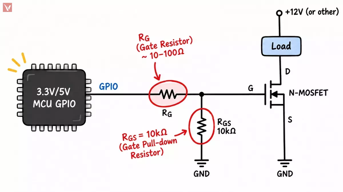
- Add a Gate-to-Source Pull-Down Resistor ( \(R_{GS}\) ): When a microcontroller boots up or enters reset, its GPIO pins default to a high-impedance (floating) state. A BJT with a floating Base naturally stays OFF because no Base current flows. A MOSFET with a floating Gate acts like an open capacitor: stray static charges or capacitive coupling can charge the Gate and turn the load ON unexpectedly. Always place a \(10\text{ k}\Omega\) to \(100\text{ k}\Omega\) pull-down resistor between Gate and Source, along with a small series gate resistor ( \(10\,\Omega\) to \(100\,\Omega\) ) to limit peak charging current and damp parasitic ringing.
- Recalculate Gate Drive Voltage: In an existing BJT circuit, the Base is often driven through a series current-limiting resistor that drops the voltage at the Base pin to \(\approx 0.7\text{ V}\) . If you leave a large series resistor in place alongside a pull-down resistor, you create a voltage divider that may prevent the MOSFET Gate from reaching its required \(2.5\text{ V}\) to \(10\text{ V}\) saturation voltage.
- Check for Unintended Reverse Conduction via the Body Diode: If the original BJT circuit relies on the transistor blocking reverse voltage when Collector potential drops below Emitter potential, replacing it with a MOSFET will allow current to flow backward through the MOSFET's internal Source-to-Drain body diode.
Frequently Asked Questions
Why do people ask "MOSFET or transistor" if a MOSFET is already a transistor?
The phrasing comes from historical convention. Bipolar Junction Transistors (BJTs) were commercialized decades before power MOSFETs became widespread. As a result, early schematics, hobbyist guides, and component bins labeled NPN and PNP bipolar parts simply as "transistors," while newer field-effect devices were called out specifically as "MOSFETs."
Can I replace an NPN transistor with an N-channel MOSFET directly on my PCB?
Only if the surrounding circuit meets MOSFET drive requirements. Even when the physical package and pin positions match (such as Pin 1 = Base/Gate, Pin 2 = Emitter/Source, Pin 3 = Collector/Drain on many SOT-23 and TO-220 devices), you must verify that the control signal supplies enough voltage ( \(V_{GS}\)) to fully saturate the MOSFET, add a Gate-to-Source pull-down resistor so the Gate never floats when the controller is in high-impedance mode, and confirm that the MOSFET's intrinsic body diode will not cause unwanted reverse current flow.
Why does my MOSFET stay ON even after I remove the gate voltage?
A MOSFET's insulated Gate forms an internal capacitor ( \(C_{iss}\)) between the Gate and the Source/Drain terminals. Once you apply a positive voltage to turn an N-channel MOSFET on, simply disconnecting the control wire leaves the charge trapped on the Gate capacitor, keeping the conductive channel open. To force the MOSFET to turn off cleanly when the drive signal is removed, connect a \(10\text{ k}\Omega\) to \(100\text{ k}\Omega\) bleed/pull-down resistor directly between the Gate and Source terminals.
Which generates less heat in power switching: a power BJT or a power MOSFET?
In almost all low-to-medium voltage switching applications (under \(200\text{ V}\)), a power MOSFET generates drastically less heat than a power BJT. Because modern MOSFETs achieve on-state resistances ( \(R_{DS(\text{on})}\)) of just a few milliohms, their conduction voltage drop at moderate currents is measured in millivolts rather than the \(0.7\text{ V}\) to \(1.5\text{ V}\) saturation drop ( \(V_{CE(\text{sat})}\)) typical of power BJTs. Power BJTs or IGBTs only gain a thermal conduction advantage in high-voltage, high-current systems (typically above \(600\text{ V}\)) where standard silicon MOSFET resistance rises steeply.
Sourcing Discrete Transistors and Power MOSFETs for Your Next Build?
Whether your schematic calls for general-purpose NPN/PNP bipolar transistors (MMBT3904, TIP31C), compact logic-level SMD switches (2N7002, IRLML6344TRPbF), or high-current power MOSFETs (IRLZ44NPbF), verifying exact package suffixes and manufacturer lot traceability is essential for production reliability. Submit your BOM or request a quote with Vigorcomp to source authentic discrete semiconductors from leading manufacturers including Infineon, onsemi, Nexperia, Toshiba, ROHM, and STMicroelectronics.